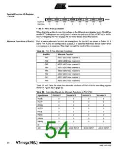
Special Function I/O Register
– SFIOR
Bit
7
ADTS2
R/W
0
6
ADTS1
R/W
0
5
ADTS0
R/W
0
4
ADHSM
R/W
0
3
ACME
R/W
0
2
1
PSR2
R/W
0
0
PSR10
R/W
0
PUD
R/W
0
SFIOR
Read/Write
Initial Value
• Bit 2 – PUD: Pull-up disable
When this bit is written to one, the pull-ups in the I/O ports are disabled even if the DDxn
and PORTxn Registers are configured to enable the pull-ups ({DDxn, PORTxn} = 0b01).
See “Configuring the Pin” on page 48 for more details about this feature.
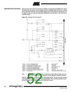
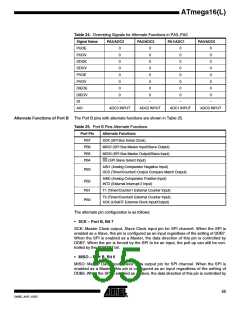
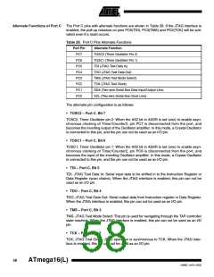
Alternate Functions of Port A Port A has an alternate function as analog input for the ADC as shown in Table 22. If
some Port A pins are configured as outputs, it is essential that these do not switch when
a conversion is in progress. This might corrupt the result of the conversion.
Table 22. Port A Pins Alternate Functions
Port Pin
PA7
Alternate Function
ADC7 (ADC input channel 7)
ADC6 (ADC input channel 6)
ADC5 (ADC input channel 5)
ADC4 (ADC input channel 4)
ADC3 (ADC input channel 3)
ADC2 (ADC input channel 2)
ADC1 (ADC input channel 1)
ADC0 (ADC input channel 0)
PA6
PA5
PA4
PA3
PA2
PA1
PA0
Table 23 and Table 24 relate the alternate functions of Port A to the overriding signals
shown in Figure 26 on page 52.
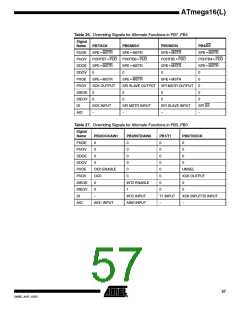
Table 23. Overriding Signals for Alternate Functions in PA7..PA4
Signal Name
PUOE
PUOV
DDOE
DDOV
PVOE
PVOV
DIEOE
DIEOV
DI
PA7/ADC7
PA6/ADC6
PA5/ADC5
PA4/ADC4
0
0
0
0
0
0
0
0
0
0
0
0
0
0
0
0
0
0
0
0
0
0
0
0
0
0
0
0
0
0
0
0
–
–
–
–
AIO
ADC7 INPUT
ADC6 INPUT
ADC5 INPUT
ADC4 INPUT
54
ATmega16(L)
2466E–AVR–10/02

 ATMEL [ ATMEL ]