from Power-down or Standby mode due to unstable clock signal upon start-up, no
matter whether the Oscillator is in use or a clock signal is applied to the TOSC1 pin.
•
•
Description of wake up from Power-save or Extended Standby mode when the timer
is clocked asynchronously: When the interrupt condition is met, the wake up
process is started on the following cycle of the timer clock, that is, the timer is
always advanced by at least one before the processor can read the counter value.
After wake-up, the MCU is halted for four cycles, it executes the interrupt routine,
and resumes execution from the instruction following SLEEP.
Reading of the TCNT2 Register shortly after wake-up from Power-save may give an
incorrect result. Since TCNT2 is clocked on the asynchronous TOSC clock, reading
TCNT2 must be done through a register synchronized to the internal I/O clock
domain. Synchronization takes place for every rising TOSC1 edge. When waking up
from Power-save mode, and the I/O clock (clkI/O) again becomes active, TCNT2 will
read as the previous value (before entering sleep) until the next rising TOSC1 edge.
The phase of the TOSC clock after waking up from Power-save mode is essentially
unpredictable, as it depends on the wake-up time. The recommended procedure for
reading TCNT2 is thus as follows:
1. Write any value to either of the registers OCR2 or TCCR2.
2. Wait for the corresponding Update Busy Flag to be cleared.
3. Read TCNT2.
•
During asynchronous operation, the synchronization of the interrupt flags for the
asynchronous timer takes three processor cycles plus one timer cycle. The timer is
therefore advanced by at least one before the processor can read the timer value
causing the setting of the interrupt flag. The output compare pin is changed on the
timer clock and is not synchronized to the processor clock.
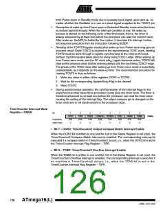
Timer/Counter Interrupt Mask
Register – TIMSK
Bit
7
OCIE2
R/W
0
6
TOIE2
R/W
0
5
TICIE1
R/W
0
4
OCIE1A
R/W
0
3
OCIE1B
R/W
0
2
TOIE1
R/W
0
1
OCIE0
R/W
0
0
TOIE0
R/W
0
TIMSK
Read/Write
Initial Value
• Bit 7 – OCIE2: Timer/Counter2 Output Compare Match Interrupt Enable
When the OCIE2 bit is written to one and the I-bit in the Status Register is set (one), the
Timer/Counter2 Compare Match interrupt is enabled. The corresponding interrupt is
executed if a compare match in Timer/Counter2 occurs, i.e., when the OCF2 bit is set in
the Timer/Counter Interrupt Flag Register – TIFR.
• Bit 6 – TOIE2: Timer/Counter2 Overflow Interrupt Enable
When the TOIE2 bit is written to one and the I-bit in the Status Register is set (one), the
Timer/Counter2 Overflow interrupt is enabled. The corresponding interrupt is executed if
an overflow in Timer/Counter2 occurs, i.e., when the TOV2 bit is set in the
Timer/Counter Interrupt Flag Register – TIFR.
126
ATmega16(L)
2466E–AVR–10/02

 ATMEL [ ATMEL ]