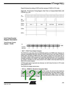
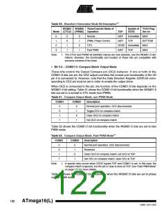
Table 50. Waveform Generation Mode Bit Description(1)
WGM21 WGM20 Timer/Counter Mode of
Update of TOV2 Flag
OCR2 Set on
Mode
(CTC2)
(PWM2) Operation
TOP
0xFF
0xFF
0
1
2
3
0
0
1
1
0
1
0
1
Normal
Immediate MAX
TOP BOTTOM
PWM, Phase Correct
CTC
OCR2 Immediate MAX
0xFF TOP MAX
Fast PWM
Note:
1. The CTC2 and PWM2 bit definition names are now obsolete. Use the WGM21:0 def-
initions. However, the functionality and location of these bits are compatible with
previous versions of the timer.
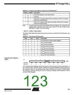
• Bit 5:4 – COM21:0: Compare Match Output Mode
These bits control the Output Compare pin (OC2) behavior. If one or both of the
COM21:0 bits are set, the OC2 output overrides the normal port functionality of the I/O
pin it is connected to. However, note that the Data Direction Register (DDR) bit corre-
sponding to OC2 pin must be set in order to enable the output driver.
When OC2 is connected to the pin, the function of the COM21:0 bits depends on the
WGM21:0 bit setting. Table 51 shows the COM21:0 bit functionality when the WGM21:0
bits are set to a normal or CTC mode (non-PWM).
Table 51. Compare Output Mode, non-PWM Mode
COM21
COM20
Description
0
0
1
1
0
1
0
1
Normal port operation, OC2 disconnected.
Toggle OC2 on compare match
Clear OC2 on compare match
Set OC2 on compare match
Table 52 shows the COM21:0 bit functionality when the WGM21:0 bits are set to fast
PWM mode.
Table 52. Compare Output Mode, Fast PWM Mode(1)
COM21
COM20
Description
0
0
1
1
0
1
0
1
Normal port operation, OC2 disconnected.
Reserved
Clear OC2 on compare match, set OC2 at TOP
Set OC2 on compare match, clear OC2 at TOP
Note:
1. A special case occurs when OCR2 equals TOP and COM21 is set. In this case, the
compare match is ignored, but the set or clear is done at TOP. See “Fast PWM Mode”
on page 117 for more details.
Table 53 shows the COM21:0 bit functionality when the WGM21:0 bits are set to phase
correct PWM mode
122
ATmega16(L)
2466E–AVR–10/02

 ATMEL [ ATMEL ]