ATmega16(L)
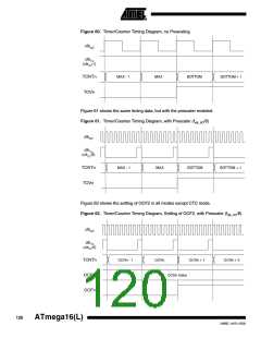
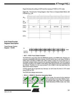
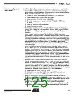
Figure 63 shows the setting of OCF2 and the clearing of TCNT2 in CTC mode.
Figure 63. Timer/Counter Timing Diagram, Clear Timer on Compare Match Mode, with
Prescaler (fclk_I/O/8)
clkI/O
clkTn
clkI/O/8)
CNTn
CTC)
TOP - 1
TOP
BOTTOM
BOTTOM + 1
OCRn
TOP
OCFn
8-bit Timer/Counter
Register Description
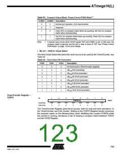
Timer/Counter Control
Register – TCCR2
Bit
7
6
5
COM21
R/W
0
4
COM20
R/W
0
3
WGM21
R/W
0
2
1
CS21
R/W
0
0
FOC2
WGM20
R/W
0
CS22
R/W
0
CS20
R/W
0
TCCR2
Read/Write
Initial Value
W
0
• Bit 7 – FOC2: Force Output Compare
The FOC2 bit is only active when the WGM bits specify a non-PWM mode. However, for
ensuring compatibility with future devices, this bit must be set to zero when TCCR2 is
written when operating in PWM mode. When writing a logical one to the FOC2 bit, an
immediate compare match is forced on the waveform generation unit. The OC2 output is
changed according to its COM21:0 bits setting. Note that the FOC2 bit is implemented
as a strobe. Therefore it is the value present in the COM21:0 bits that determines the
effect of the forced compare.
A FOC2 strobe will not generate any interrupt, nor will it clear the timer in CTC mode
using OCR2 as TOP.
The FOC2 bit is always read as zero.
• Bit 6, 3 – WGM21:0: Waveform Generation Mode
These bits control the counting sequence of the counter, the source for the maximum
(TOP) counter value, and what type of waveform generation to be used. Modes of oper-
ation supported by the Timer/Counter unit are: Normal mode, Clear Timer on Compare
match (CTC) mode, and two types of Pulse Width Modulation (PWM) modes. See Table
50 and “Modes of Operation” on page 115.
121
2466E–AVR–10/02

 ATMEL [ ATMEL ]