ATmega8U2/16U2/32U2
2.2.5
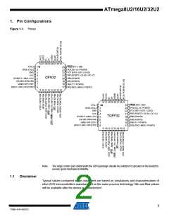
Port C (PC7..PC0)
Port C is an 8-bit bi-directional I/O port with internal pull-up resistors (selected for each bit). The
Port C output buffers have symmetrical drive characteristics with both high sink and source
capability. As inputs, Port C pins that are externally pulled low will source current if the pull-up
resistors are activated. The Port C pins are tri-stated when a reset condition becomes active,
even if the clock is not running.
Port C also serves the functions of various special features of the ATmega8U2/16U2/32U2 as
listed on page 77.
2.2.6
Port D (PD7..PD0)
Port D serves as analog inputs to the analog comparator.
Port D also serves as an 8-bit bi-directional I/O port, if the analog comparator is not used (con-
cerns PD2/PD1 pins). Port pins can provide internal pull-up resistors (selected for each bit). The
Port D output buffers have symmetrical drive characteristics with both high sink and source
capability. As inputs, Port D pins that are externally pulled low will source current if the pull-up
resistors are activated. The Port D pins are tri-stated when a reset condition becomes active,
even if the clock is not running.
2.2.7
2.2.8
2.2.9
2.2.10
2.2.11
D-
USB Full Speed Negative Data Upstream Port
USB Full Speed Positive Data Upstream Port
USB Ground.
D+
UGND
UVCC
UCAP
USB Pads Internal Regulator Input supply voltage.
USB Pads Internal Regulator Output supply voltage. Should be connected to an external capac-
itor (1μF).
2.2.12
RESET/PC1/dW
Reset input. A low level on this pin for longer than the minimum pulse length will generate a
reset, even if the clock is not running. The minimum pulse length is given in “System Control and
Reset” on page 47. Shorter pulses are not guaranteed to generate a reset. This pin alternatively
serves as debugWire channel or as generic I/O. The configuration depends on the fuses RST-
DISBL and DWEN.
2.2.13
2.2.14
XTAL1
Input to the inverting Oscillator amplifier and input to the internal clock operating circuit.
Output from the inverting Oscillator amplifier if enabled by Fuse. Also serves as a generic I/O.
XTAL2/PC0
5
7799E–AVR–09/2012

 ATMEL [ ATMEL ]