ATmega8U2/16U2/32U2
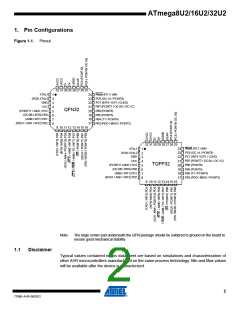
1. Pin Configurations
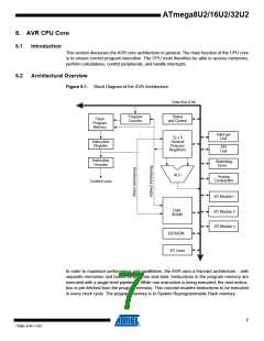
Figure 1-1. Pinout
32 31 30 29 28 27 26 25
Reset (PC1 / dW)
XTAL1
(PC0) XTAL2
GND
1
2
3
4
5
6
7
8
24
23
22
21
20
19
18
17
PC6 (OC.1A / PCINT8)
PC7 (INT4 / ICP1 / CLKO)
PB7 (PCINT7 / OC.0A / OC.1C)
VCC
(PCINT11 / AIN2 ) PC2
(OC.0B / INT0) PD0
QFN32
PB6 (PCINT6)
PB5 (PCINT5)
(AIN0 / INT1) PD1
PB4 (T1 / PCINT4)
PB3 (PDO / MISO / PCINT3)
(RXD1 / AIN1 / INT2) PD2
9 10 11 12 13 14 15 16
32 31 30 29 28 27 26 25
Reset (PC1 / dW)
24
PC6 (OC.1A / PCINT8)
23
XTAL1
1
2
3
4
5
6
7
8
(PC0) XTAL2
GND
PC7 (INT4 / ICP1 / CLKO)
PB7 (PCINT7 / OC.0A / OC.1C)
PB6 (PCINT6)
22
21
20
19
18
17
VCC
(PCINT11 /AIN2 ) PC2
(OC.0B / INT0) PD0
TQFP32
PB5 (PCINT5)
(AIN0 / INT1) PD1
PB4 (T1 / PCINT4)
(RXD1 / AIN1 / INT2) PD2
PB3 (PDO / MISO / PCINT3)
9 10 11 12 13 14 15 16
Note:
The large center pad underneath the QFN package should be soldered to ground on the board to
ensure good mechanical stability.
1.1
Disclaimer
Typical values contained in this datasheet are based on simulations and characterization of
other AVR microcontrollers manufactured on the same process technology. Min and Max values
will be available after the device is characterized.
2
7799E–AVR–09/2012

 ATMEL [ ATMEL ]