ATmega8U2/16U2/32U2
enabled and the input signal is left floating or have an analog signal level close to VCC/2, the
input buffer will use excessive power.
For analog input pins, the digital input buffer should be disabled at all times. An analog signal
level close to VCC/2 on an input pin can cause significant current even in active mode. Digital
input buffers can be disabled by writing to the Digital Input Disable Registers (DIDR1). Refer to
“DIDR1 – Digital Input Disable Register 1” on page 225 for details.
9.9.6
On-chip Debug System
If the On-chip debug system is enabled by the OCDEN Fuse and the chip enters sleep mode,
the main clock source is enabled, and hence, always consumes power. In the deeper sleep
modes, this will contribute significantly to the total current consumption.
9.10 Register Description
9.10.1
SMCR – Sleep Mode Control Register
The Sleep Mode Control Register contains control bits for power management.
Bit
7
–
6
–
5
–
4
–
3
2
1
0
SE
R/W
0
0x33 (0x53)
Read/Write
Initial Value
SM2
R/W
0
SM1
R/W
0
SM0
R/W
0
SMCR
R
0
R
0
R
0
R
0
• Bit 7:4 - Reserved bits
These bits are reserved and will always read as zero.
• Bits 3:1 – SM[2:0]: Sleep Mode Select Bits 2, 1, and 0
These bits select between the five available sleep modes as shown in Table 9-2.
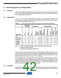
Table 9-2.
Sleep Mode Select
SM2
SM1
SM0
Sleep Mode
Idle
0
0
0
0
1
1
1
1
0
0
1
1
0
0
1
1
0
1
0
1
0
1
0
1
Reserved
Power-down
Power-save
Reserved
Reserved
Standby(1)
Extended Standby(1)
Note: 1. Standby modes are only recommended for use with external crystals or resonators.
• Bit 0– SE: Sleep Enable
The SE bit must be written to logic one to make the MCU enter the sleep mode when the SLEEP
instruction is executed. To avoid the MCU entering the sleep mode unless it is the programmer’s
purpose, it is recommended to write the Sleep Enable (SE) bit to one just before the execution of
the SLEEP instruction and to clear it immediately after waking up.
45
7799D–AVR–11/10

 ATMEL [ ATMEL ]