ATmega8U2/16U2/32U2
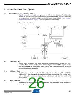
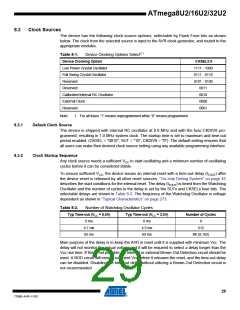
8.3
Clock Sources
The device has the following clock source options, selectable by Flash Fuse bits as shown
below. The clock from the selected source is input to the AVR clock generator, and routed to the
appropriate modules.
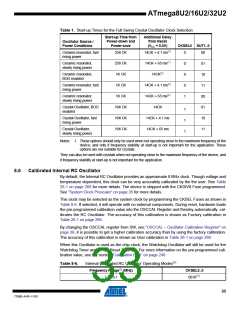
Table 8-1.
Device Clocking Options Select(1)
Device Clocking Option
Low Power Crystal Oscillator
Full Swing Crystal Oscillator
Reserved
CKSEL3:0
1111 - 1000
0111 - 0110
0101 - 0100
0011
Reserved
Calibrated Internal RC Oscillator
External Clock
0010
0000
Reserved
0001
Note:
1. For all fuses “1” means unprogrammed while “0” means programmed.
8.3.1
8.3.2
Default Clock Source
The device is shipped with internal RC oscillator at 8.0 MHz and with the fuse CKDIV8 pro-
grammed, resulting in 1.0 MHz system clock. The startup time is set to maximum and time-out
period enabled. (CKSEL = "0010", SUT = "10", CKDIV8 = "0"). The default setting ensures that
all users can make their desired clock source setting using any available programming interface.
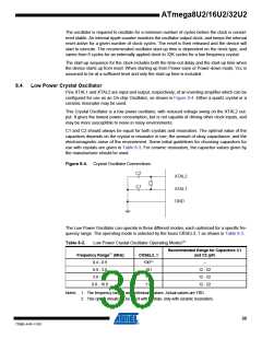
Clock Startup Sequence
Any clock source needs a sufficient VCC to start oscillating and a minimum number of oscillating
cycles before it can be considered stable.
To ensure sufficient VCC, the device issues an internal reset with a time-out delay (tTOUT) after
the device reset is released by all other reset sources. “On-chip Debug System” on page 45
describes the start conditions for the internal reset. The delay (tTOUT) is timed from the Watchdog
Oscillator and the number of cycles in the delay is set by the SUTx and CKSELx fuse bits. The
selectable delays are shown in Table 8-2. The frequency of the Watchdog Oscillator is voltage
dependent as shown in “Typical Characteristics” on page 273.
Table 8-2.
Number of Watchdog Oscillator Cycles
Typ Time-out (VCC = 5.0V)
0 ms
Typ Time-out (VCC = 3.0V)
0 ms
Number of Cycles
0
4.1 ms
65 ms
4.3 ms
69 ms
512
8K (8,192)
Main purpose of the delay is to keep the AVR in reset until it is supplied with minimum Vcc. The
delay will not monitor the actual voltage and it will be required to select a delay longer than the
Vcc rise time. If this is not possible, an internal or external Brown-Out Detection circuit should be
used. A BOD circuit will ensure sufficient Vcc before it releases the reset, and the time-out delay
can be disabled. Disabling the time-out delay without utilizing a Brown-Out Detection circuit is
not recommended.
29
7799D–AVR–11/10

 ATMEL [ ATMEL ]