ATmega169P
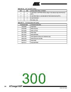
When pulsing WR or OE, the command loaded determines the action executed. The different
Commands are shown in Table 26-11.
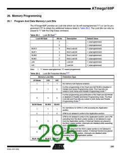
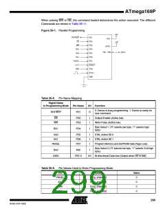
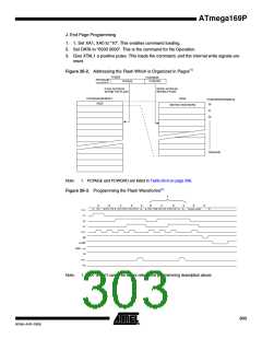
Figure 26-1. Parallel Programming
+5V
RDY/BSY
OE
PD1
PD2
PD3
PD4
PD5
PD6
PD7
VCC
+5V
WR
AVCC
BS1
PB7 - PB0
DATA
XA0
XA1
PAGEL
+12 V
BS2
RESET
PA0
XTAL1
GND
Table 26-8. Pin Name Mapping
Signal Name
in Programming Mode
Pin Name
I/O Function
0: Device is busy programming, 1: Device is ready for
new command.
RDY/BSY
PD1
O
OE
PD2
PD3
I
I
Output Enable (Active low).
Write Pulse (Active low).
WR
Byte Select 1 (“0” selects low byte, “1” selects high
byte).
BS1
PD4
I
XA0
XA1
PD5
PD6
PD7
I
I
I
XTAL Action Bit 0
XTAL Action Bit 1
PAGEL
Program Memory and EEPROM data Page Load.
Byte Select 2 (“0” selects low byte, “1” selects 2’nd high
byte).
BS2
PA0
I
DATA
PB7-0
I/O Bi-directional Data bus (Output when OE is low).
Table 26-9. Pin Values Used to Enter Programming Mode
Pin
PAGEL
XA1
Symbol
Value
Prog_enable[3]
Prog_enable[2]
Prog_enable[1]
Prog_enable[0]
0
0
0
0
XA0
BS1
299
8018A–AVR–03/06

 ATMEL [ ATMEL ]