ATmega169P
21. ADC - Analog to Digital Converter
21.1 Features
• 10-bit Resolution
• 0.5 LSB Integral Non-linearity
•
2 LSB Absolute Accuracy
• 13 µs - 260 µs Conversion Time (50 kHz to 1 MHz ADC clock)
• Up to 15 kSPS at Maximum Resolution (200 kHz ADC clock)
• Eight Multiplexed Single Ended Input Channels
• Optional Left Adjustment for ADC Result Readout
• 0 - VCC ADC Input Voltage Range
• Selectable 1.1V ADC Reference Voltage
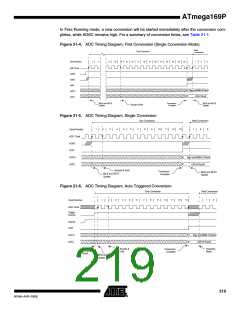
• Free Running or Single Conversion Mode
• ADC Start Conversion by Auto Triggering on Interrupt Sources
• Interrupt on ADC Conversion Complete
• Sleep Mode Noise Canceler
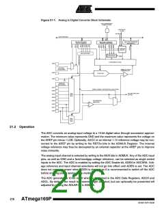
The ATmega169P features a 10-bit successive approximation ADC. The ADC is connected to
an 8-channel Analog Multiplexer which allows eight single-ended voltage inputs constructed
from the pins of Port F. The single-ended voltage inputs refer to 0V (GND).
The ADC contains a Sample and Hold circuit which ensures that the input voltage to the ADC is
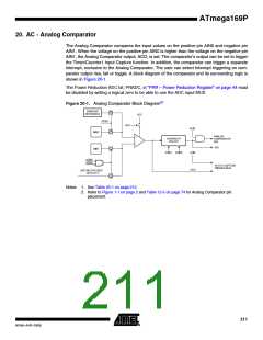
held at a constant level during conversion. A block diagram of the ADC is shown in Figure 21-1.
The ADC has a separate analog supply voltage pin, AVCC. AVCC must not differ more than
0.3V from VCC. See the paragraph ”ADC Noise Canceler” on page 221 on how to connect this
pin.
Internal reference voltages of nominally 1.1V or AVCC are provided On-chip. The voltage refer-
ence may be externally decoupled at the AREF pin by a capacitor for better noise performance.
The Power Reduction ADC bit, PRADC, in ”PRR – Power Reduction Register” on page 44 must
be written to zero to enable the ADC module.
215
8018A–AVR–03/06

 ATMEL [ ATMEL ]