ATmega169P
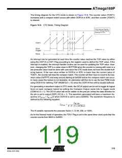
The Timer/Counter Overflow Flag (TOV1) is set each time the counter reaches BOTTOM. When
either OCR1A or ICR1 is used for defining the TOP value, the OC1A or ICF1 Flag is set accord-
ingly at the same timer clock cycle as the OCR1x Registers are updated with the double buffer
value (at TOP). The Interrupt Flags can be used to generate an interrupt each time the counter
reaches the TOP or BOTTOM value.
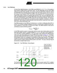
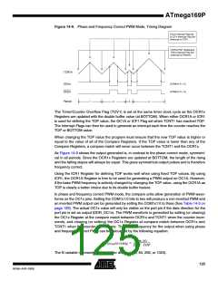
When changing the TOP value the program must ensure that the new TOP value is higher or
equal to the value of all of the Compare Registers. If the TOP value is lower than any of the
Compare Registers, a compare match will never occur between the TCNT1 and the OCR1x.
Note that when using fixed TOP values, the unused bits are masked to zero when any of the
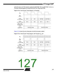
OCR1x Registers are written. As the third period shown in Figure 14-8 illustrates, changing the
TOP actively while the Timer/Counter is running in the phase correct mode can result in an
unsymmetrical output. The reason for this can be found in the time of update of the OCR1x Reg-
ister. Since the OCR1x update occurs at TOP, the PWM period starts and ends at TOP. This
implies that the length of the falling slope is determined by the previous TOP value, while the
length of the rising slope is determined by the new TOP value. When these two values differ the
two slopes of the period will differ in length. The difference in length gives the unsymmetrical
result on the output.
It is recommended to use the phase and frequency correct mode instead of the phase correct
mode when changing the TOP value while the Timer/Counter is running. When using a static
TOP value there are practically no differences between the two modes of operation.
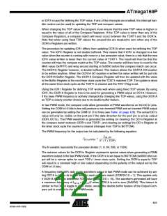
In phase correct PWM mode, the compare units allow generation of PWM waveforms on the
OC1x pins. Setting the COM1x1:0 bits to two will produce a non-inverted PWM and an inverted
PWM output can be generated by setting the COM1x1:0 to three (See Table 14-3 on page 129).
The actual OC1x value will only be visible on the port pin if the data direction for the port pin is
set as output (DDR_OC1x). The PWM waveform is generated by setting (or clearing) the OC1x
Register at the compare match between OCR1x and TCNT1 when the counter increments, and
clearing (or setting) the OC1x Register at compare match between OCR1x and TCNT1 when
the counter decrements. The PWM frequency for the output when using phase correct PWM can
be calculated by the following equation:
f
clk_I/O
f
= ---------------------------
OCnxPCPWM
2 ⋅ N ⋅ TOP
The N variable represents the prescaler divider (1, 8, 64, 256, or 1024).
The extreme values for the OCR1x Register represent special cases when generating a PWM
waveform output in the phase correct PWM mode. If the OCR1x is set equal to BOTTOM the
output will be continuously low and if set equal to TOP the output will be continuously high for
non-inverted PWM mode. For inverted PWM the output will have the opposite logic values. If
OCR1A is used to define the TOP value (WGM13:0 = 11) and COM1A1:0 = 1, the OC1A output
will toggle with a 50ꢀ duty cycle.
123
8018A–AVR–03/06

 ATMEL [ ATMEL ]