14.8.4
Phase Correct PWM Mode
The phase correct Pulse Width Modulation or phase correct PWM mode (WGM13:0 = 1, 2, 3,
10, or 11) provides a high resolution phase correct PWM waveform generation option. The
phase correct PWM mode is, like the phase and frequency correct PWM mode, based on a dual-
slope operation. The counter counts repeatedly from BOTTOM (0x0000) to TOP and then from
TOP to BOTTOM. In non-inverting Compare Output mode, the Output Compare (OC1x) is
cleared on the compare match between TCNT1 and OCR1x while upcounting, and set on the
compare match while downcounting. In inverting Output Compare mode, the operation is
inverted. The dual-slope operation has lower maximum operation frequency than single slope
operation. However, due to the symmetric feature of the dual-slope PWM modes, these modes
are preferred for motor control applications.
The PWM resolution for the phase correct PWM mode can be fixed to 8-, 9-, or 10-bit, or defined
by either ICR1 or OCR1A. The minimum resolution allowed is 2-bit (ICR1 or OCR1A set to
0x0003), and the maximum resolution is 16-bit (ICR1 or OCR1A set to MAX). The PWM resolu-
tion in bits can be calculated by using the following equation:
log(TOP + 1)
R
= ----------------------------------
PCPWM
log(2)
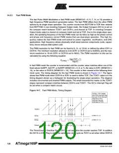
In phase correct PWM mode the counter is incremented until the counter value matches either
one of the fixed values 0x00FF, 0x01FF, or 0x03FF (WGM13:0 = 1, 2, or 3), the value in ICR1
(WGM13:0 = 10), or the value in OCR1A (WGM13:0 = 11). The counter has then reached the
TOP and changes the count direction. The TCNT1 value will be equal to TOP for one timer clock
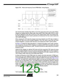
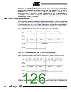
cycle. The timing diagram for the phase correct PWM mode is shown on Figure 14-8. The figure
shows phase correct PWM mode when OCR1A or ICR1 is used to define TOP. The TCNT1
value is in the timing diagram shown as a histogram for illustrating the dual-slope operation. The
diagram includes non-inverted and inverted PWM outputs. The small horizontal line marks on
the TCNT1 slopes represent compare matches between OCR1x and TCNT1. The OC1x Inter-
rupt Flag will be set when a compare match occurs.
Figure 14-8. Phase Correct PWM Mode, Timing Diagram
OCRnx/TOP Update and
OCnA Interrupt Flag Set
or ICFn Interrupt Flag Set
(Interrupt on TOP)
TOVn Interrupt Flag Set
(Interrupt on Bottom)
TCNTn
(COMnx1:0 = 2)
OCnx
(COMnx1:0 = 3)
OCnx
1
2
3
4
Period
122
ATmega169P
8018A–AVR–03/06

 ATMEL [ ATMEL ]