ering is disabled. The double buffering synchronizes the update of the OCR2 Compare Register
to either top or bottom of the counting sequence. The synchronization prevents the occurrence
of odd-length, non-symmetrical PWM pulses, thereby making the output glitch-free.
The OCR2 Register access may seem complex, but this is not case. When the double buffering
is enabled, the CPU has access to the OCR2 buffer Register, and if double buffering is disabled
the CPU will access the OCR2 directly.
Force Output
Compare
In non-PWM Waveform Generation modes, the match output of the comparator can be forced by
writing a one to the force output compare (FOC2) bit. Forcing compare match will not set the
OCF2 flag or reload/clear the timer, but the OC2 pin will be updated as if a real compare match
had occurred (the COM21:0 bits settings define whether the OC2 pin is set, cleared or toggled).
Compare Match
Blocking by TCNT2
Write
All CPU write operations to the TCNT2 Register will block any compare match that occur in the
next timer clock cycle, even when the timer is stopped. This feature allows OCR2 to be initialized
to the same value as TCNT2 without triggering an interrupt when the Timer/Counter clock is
enabled.
Using the Output
Compare Unit
Since writing TCNT2 in any mode of operation will block all compare matches for one timer clock
cycle, there are risks involved when changing TCNT2 when using the output compare channel,
independently of whether the Timer/Counter is running or not. If the value written to TCNT2
equals the OCR2 value, the compare match will be missed, resulting in incorrect waveform gen-
eration. Similarly, do not write the TCNT2 value equal to BOTTOM when the counter is
downcounting.
The setup of the OC2 should be performed before setting the Data Direction Register for the port
pin to output. The easiest way of setting the OC2 value is to use the Force Output Compare
(FOC2) strobe bits in normal mode. The OC2 Register keeps its value even when changing
between waveform generation modes.
Be aware that the COM21:0 bits are not double buffered together with the compare value.
Changing the COM21:0 bits will take effect immediately.
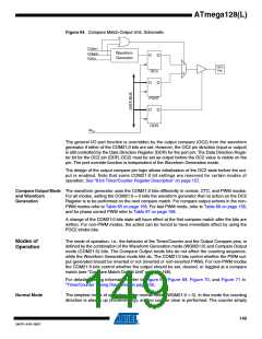
Compare Match
Output Unit
The Compare Output mode (COM21:0) bits have two functions. The waveform generator uses
the COM21:0 bits for defining the output compare (OC2) state at the next compare match. Also,
the COM21:0 bits control the OC2 pin output source. Figure 64 shows a simplified schematic of
the logic affected by the COM21:0 bit setting. The I/O registers, I/O bits, and I/O pins in the fig-
ure are shown in bold. Only the parts of the general I/O Port Control Registers (DDR and PORT)
that are affected by the COM21:0 bits are shown. When referring to the OC2 state, the reference
is for the internal OC2 Register, not the OC2 pin. If a System Reset occur, the OC2 Register is
reset to “0”.
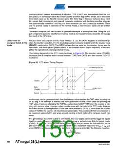
148
ATmega128(L)
2467P–AVR–08/07

 ATMEL [ ATMEL ]