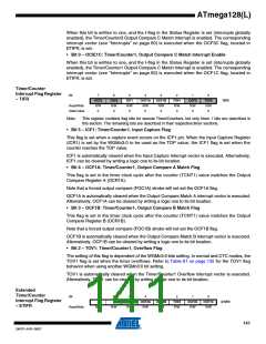
ATmega128(L)
8-bit
Timer/Counter2
with PWM
Timer/Counter2 is a general purpose, single channel, 8-bit Timer/Counter module. The main
features are:
• Single Channel Counter
• Clear Timer on Compare Match (Auto Reload)
• Glitch-free, Phase Correct Pulse width Modulator (PWM)
• Frequency Generator
• External Event Counter
• 10-bit Clock Prescaler
• Overflow and Compare Match Interrupt Sources (TOV2 and OCF2)
Overview
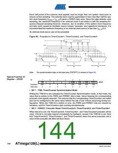
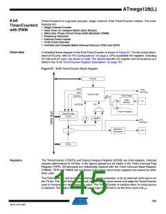
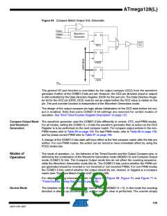
A simplified block diagram of the 8-bit Timer/Counter is shown in Figure 61. For the actual place-
ment of I/O pins, refer to “Pin Configurations” on page 2. CPU accessible I/O registers, including
I/O bits and I/O pins, are shown in bold. The device-specific I/O register and bit locations are
listed in the “8-bit Timer/Counter Register Description” on page 157.
Figure 61. 8-Bit Timer/Counter Block Diagram
TCCRn
count
TOVn
(Int.Req.)
clear
Control Logic
TOP
Clock Select
direction
clk
Tn
Edge
Detector
Tn
BOTTOM
( From Prescaler )
Timer/Counter
TCNTn
= 0
= 0xFF
OCn
(Int.Req.)
Waveform
Generation
OCn
=
OCRn
Registers
The Timer/Counter (TCNT2) and Output Compare Register (OCR2) are 8-bit registers. Interrupt
request (abbreviated to Int.Req. in the figure) signals are all visible in the Timer Interrupt Flag
Register (TIFR). All interrupts are individually masked with the Timer Interrupt Mask Register
(TIMSK). TIFR and TIMSK are not shown in the figure since these registers are shared by other
timer units.
The Timer/Counter can be clocked internally, via the prescaler, or by an external clock source on
the T2 pin. The Clock Select logic block controls which clock source and edge the Timer/Counter
uses to increment (or decrement) its value. The Timer/Counter is inactive when no clock source
is selected. The output from the clock select logic is referred to as the timer clock (clkT2).
145
2467P–AVR–08/07

 ATMEL [ ATMEL ]