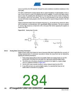
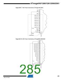
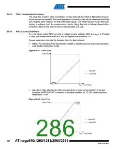
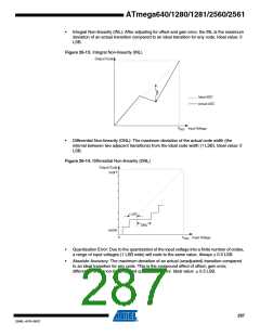
26.7 ADC Conversion Result
After the conversion is complete (ADIF is high), the conversion result can be found in the ADC
Result Registers (ADCL, ADCH).
For single ended conversion, the result is
V
⋅ 1024
IN
ADC = --------------------------
V
REF
where VIN is the voltage on the selected input pin and VREF the selected voltage reference (see
Table 26-3 on page 290 and Table 26-4 on page 291). 0x000 represents analog ground, and
0x3FF represents the selected reference voltage minus one LSB.
If differential channels are used, the result is
(V
– V
) ⋅ 512
NEG
POS
ADC = ----------------------------------------------------
V
REF
where VPOS is the voltage on the positive input pin, VNEG the voltage on the negative input pin,
and VREF the selected voltage reference. The result is presented in two’s complement form, from
0x200 (-512d) through 0x1FF (+511d). Note that if the user wants to perform a quick polarity
check of the result, it is sufficient to read the MSB of the result (ADC9 in ADCH). If the bit is one,
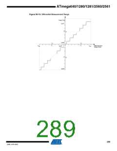
the result is negative, and if this bit is zero, the result is positive. Figure 26-15 shows the decod-
ing of the differential input range.
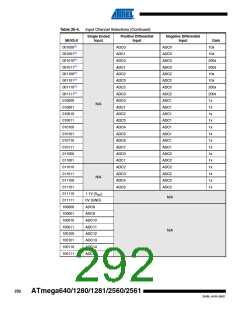
Table 26-2 shows the resulting output codes if the differential input channel pair (ADCn - ADCm)
is selected with a gain of GAIN and a reference voltage of VREF
.
288
ATmega640/1280/1281/2560/2561
2549L–AVR–08/07

 ATMEL [ ATMEL ]