•
•
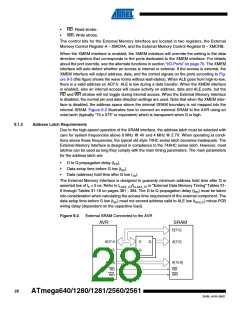
RD: Read strobe.
WR: Write strobe.
The control bits for the External Memory Interface are located in two registers, the External
Memory Control Register A – XMCRA, and the External Memory Control Register B – XMCRB.
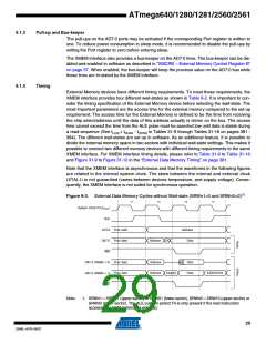
When the XMEM interface is enabled, the XMEM interface will override the setting in the data
direction registers that corresponds to the ports dedicated to the XMEM interface. For details
about the port override, see the alternate functions in section “I/O-Ports” on page 70. The XMEM
interface will auto-detect whether an access is internal or external. If the access is external, the
XMEM interface will output address, data, and the control signals on the ports according to Fig-
ure 9-3 (this figure shows the wave forms without wait-states). When ALE goes from high-to-low,
there is a valid address on AD7:0. ALE is low during a data transfer. When the XMEM interface
is enabled, also an internal access will cause activity on address, data and ALE ports, but the
RD and WR strobes will not toggle during internal access. When the External Memory Interface
is disabled, the normal pin and data direction settings are used. Note that when the XMEM inter-
face is disabled, the address space above the internal SRAM boundary is not mapped into the
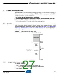
internal SRAM. Figure 9-2 illustrates how to connect an external SRAM to the AVR using an
octal latch (typically “74 x 573” or equivalent) which is transparent when G is high.
9.1.2
Address Latch Requirements
Due to the high-speed operation of the XRAM interface, the address latch must be selected with
care for system frequencies above 8 MHz @ 4V and 4 MHz @ 2.7V. When operating at condi-
tions above these frequencies, the typical old style 74HC series latch becomes inadequate. The
External Memory Interface is designed in compliance to the 74AHC series latch. However, most
latches can be used as long they comply with the main timing parameters. The main parameters
for the address latch are:
•
•
•
D to Q propagation delay (tPD).
Data setup time before G low (tSU).
Data (address) hold time after G low (TH).
The External Memory Interface is designed to guaranty minimum address hold time after G is
asserted low of th = 5 ns. Refer to tLAXX_LD/tLLAXX_ST in “External Data Memory Timing” Tables 31-
9 through Tables 31-16 on pages 381 - 384. The D-to-Q propagation delay (tPD) must be taken
into consideration when calculating the access time requirement of the external component. The
data setup time before G low (tSU) must not exceed address valid to ALE low (tAVLLC) minus PCB
wiring delay (dependent on the capacitive load).
Figure 9-2. External SRAM Connected to the AVR
AVR
SRAM
D[7:0]
AD7:0
D
G
Q
A[7:0]
ALE
A[15:8]
A15:8
RD
RD
WR
WR
28
ATmega640/1280/1281/2560/2561
2549L–AVR–08/07

 ATMEL [ ATMEL ]