AT90PWM2/3/2B/3B
Each half period of the external clock applied must be longer than one system clock cycle to
ensure correct sampling. The external clock must be guaranteed to have less than half the sys-
tem clock frequency (fExtClk < fclk_I/O/2) given a 50/50% duty cycle. Since the edge detector uses
sampling, the maximum frequency of an external clock it can detect is half the sampling fre-
quency (Nyquist sampling theorem). However, due to variation of the system clock frequency
and duty cycle caused by Oscillator source (crystal, resonator, and capacitors) tolerances, it is
recommended that maximum frequency of an external clock source is less than fclk_I/O/2.5.
An external clock source can not be prescaled.
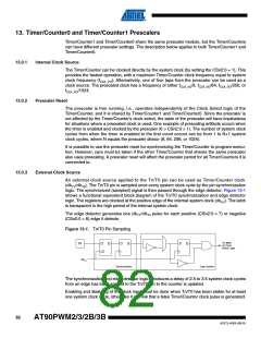
Figure 13-2. Prescaler for Timer/Counter0 and Timer/Counter1(1)
clkI/O
Clear
PSRSYNC
T0
Synchronization
T1
Synchronization
clkT1
clkT0
Note:
1. The synchronization logic on the input pins (Tn/T0) is shown in Figure 13-1.
13.0.4
General Timer/Counter Control Register – GTCCR
Bit
7
6
ICPSEL1
R/W
5
–
4
–
3
–
2
–
1
–
0
PSRSYNC
R/W
TSM
R/W
0
GTCCR
Read/Write
Initial Value
R
0
R
0
R
0
R
0
R
0
0
0
• Bit 7 – TSM: Timer/Counter Synchronization Mode
Writing the TSM bit to one activates the Timer/Counter Synchronization mode. In this mode, the
value that is written to the PSRSYNC bit is kept, hence keeping the corresponding prescaler
reset signals asserted. This ensures that the corresponding Timer/Counters are halted and can
be configured to the same value without the risk of one of them advancing during configuration.
When the TSM bit is written to zero, the PSRSYNC bit is cleared by hardware, and the
Timer/Counters start counting simultaneously.
• Bit6 – ICPSEL1: Timer 1 Input Capture selection
83
4317J–AVR–08/10

 ATMEL [ ATMEL ]