The definitions in Table 14-1 are also used extensively throughout the document.
Table 14-1. Definitions
BOTTOM
MAX
The counter reaches the BOTTOM when it becomes 0x00.
The counter reaches its MAXimum when it becomes 0xFF (decimal 255).
TOP
The counter reaches the TOP when it becomes equal to the highest value in the
count sequence. The TOP value can be assigned to be the fixed value 0xFF
(MAX) or the value stored in the OCR0A Register. The assignment is depen-
dent on the mode of operation.
14.1.2
Registers
The Timer/Counter (TCNT0) and Output Compare Registers (OCR0A and OCR0B) are 8-bit
registers. Interrupt request (abbreviated to Int.Req. in the figure) signals are all visible in the
Timer Interrupt Flag Register (TIFR0). All interrupts are individually masked with the Timer Inter-
rupt Mask Register (TIMSK0). TIFR0 and TIMSK0 are not shown in the figure.
The Timer/Counter can be clocked internally, via the prescaler, or by an external clock source on
the T0 pin. The Clock Select logic block controls which clock source and edge the Timer/Counter
uses to increment (or decrement) its value. The Timer/Counter is inactive when no clock source
is selected. The output from the Clock Select logic is referred to as the timer clock (clkT0).
The double buffered Output Compare Registers (OCR0A and OCR0B) are compared with the
Timer/Counter value at all times. The result of the compare can be used by the Waveform Gen-
erator to generate a PWM or variable frequency output on the Output Compare pins (OC0A and
OC0B). See “Using the Output Compare Unit” on page 112. for details. The compare match
event will also set the Compare Flag (OCF0A or OCF0B) which can be used to generate an Out-
put Compare interrupt request.
14.2 Timer/Counter Clock Sources
The Timer/Counter can be clocked by an internal or an external clock source. The clock source
is selected by the Clock Select logic which is controlled by the Clock Select (CS02:0) bits
located in the Timer/Counter Control Register (TCCR0B). For details on clock sources and pres-
caler, see “Timer/Counter0 and Timer/Counter1 Prescalers” on page 82.
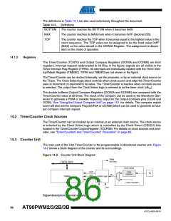
14.3 Counter Unit
The main part of the 8-bit Timer/Counter is the programmable bi-directional counter unit. Figure
14-2 shows a block diagram of the counter and its surroundings.
Figure 14-2. Counter Unit Block Diagram
TOVn
(Int.Req.)
DATA BUS
Clock Select
count
clear
Edge
Detector
Tn
clkTn
TCNTn
Control Logic
direction
( From Prescaler )
bottom
top
Signal description (internal signals):
86
AT90PWM2/3/2B/3B
4317J–AVR–08/10

 ATMEL [ ATMEL ]