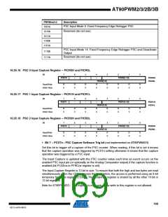
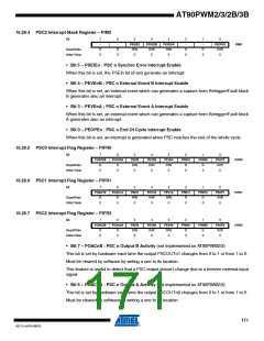
AT90PWM2/3/2B/3B
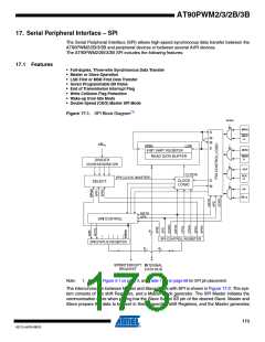
17. Serial Peripheral Interface – SPI
The Serial Peripheral Interface (SPI) allows high-speed synchronous data transfer between the
AT90PWM2/2B/3/3B and peripheral devices or between several AVR devices.
The AT90PWM2/2B/3/3B SPI includes the following features:
17.1 Features
• Full-duplex, Three-wire Synchronous Data Transfer
• Master or Slave Operation
• LSB First or MSB First Data Transfer
• Seven Programmable Bit Rates
• End of Transmission Interrupt Flag
• Write Collision Flag Protection
• Wake-up from Idle Mode
• Double Speed (CK/2) Master SPI Mode
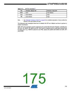
Figure 17-1. SPI Block Diagram(1)
SPIPS
MISO
MISO
_A
clkIO
MOSI
MOSI
_A
DIVIDER
/2/4/8/16/32/64/128
SCK
SCK
_A
SS
SS_A
Note:
1. Refer to Figure 3-1 on page 3, and Table 11-3 on page 68 for SPI pin placement.
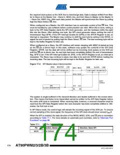
The interconnection between Master and Slave CPUs with SPI is shown in Figure 17-2. The sys-
tem consists of two shift Registers, and a Master clock generator. The SPI Master initiates the
communication cycle when pulling low the Slave Select SS pin of the desired Slave. Master and
Slave prepare the data to be sent in their respective shift Registers, and the Master generates
173
4317J–AVR–08/10

 ATMEL [ ATMEL ]