AT90USB82/162
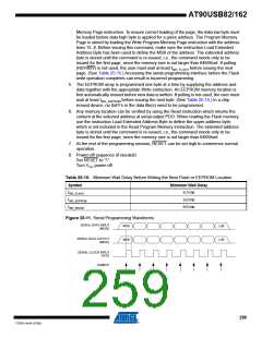
Memory Page instruction. To ensure correct loading of the page, the data low byte must
be loaded before data high byte is applied for a given address. The Program Memory
Page is stored by loading the Write Program Memory Page instruction with the address
lines 15..8. Before issuing this command, make sure the instruction Load Extended
Address Byte has been used to define the MSB of the address. The extended address
byte is stored until the command is re-issued, i.e., the command needs only to be
issued for the first page, since the memory size is not larger than 64KWord. If polling
(RDY/BSY) is not used, the user must wait at least tWD_FLASH before issuing the next
page. (See Table 25-15.) Accessing the serial programming interface before the Flash
write operation completes can result in incorrect programming.
5. The EEPROM array is programmed one byte at a time by supplying the address and
data together with the appropriate Write instruction. An EEPROM memory location is
first automatically erased before new data is written. If polling is not used, the user must
wait at least tWD_EEPROM before issuing the next byte. (See Table 25-15.) In a chip
erased device, no 0xFFs in the data file(s) need to be programmed.
6. Any memory location can be verified by using the Read instruction which returns the
content at the selected address at serial output PDO. When reading the Flash memory,
use the instruction Load Extended Address Byte to define the upper address byte,
which is not included in the Read Program Memory instruction. The extended address
byte is stored until the command is re-issued, i.e., the command needs only to be
issued for the first page, since the memory size is not larger than 64KWord.
7. At the end of the programming session, RESET can be set high to commence normal
operation.
8. Power-off sequence (if needed):
Set RESET to “1”.
Turn VCC power off.
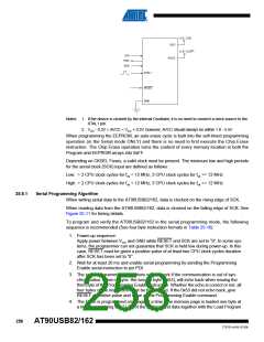
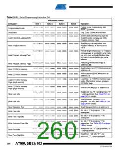
Table 25-15. Minimum Wait Delay Before Writing the Next Flash or EEPROM Location
Symbol
Minimum Wait Delay
4.5 ms
tWD_FLASH
tWD_EEPROM
tWD_ERASE
9.0 ms
9.0 ms
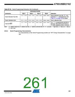
Figure 25-11. Serial Programming Waveforms
SERIAL DATA INPUT
MSB
LSB
LSB
(MOSI)
SERIAL DATA OUTPUT
MSB
(MISO)
SERIAL CLOCK INPUT
(SCK)
SAMPLE
259
7707D–AVR–07/08

 ATMEL [ ATMEL ]