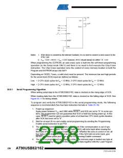
+1.8 - 5.5V
VCC
+1.8 - 5.5V(2)
PDI
AVCC
PDO
SCK
XTAL1
RESET
GND
Notes: 1. If the device is clocked by the internal Oscillator, it is no need to connect a clock source to the
XTAL1 pin.
2. VCC - 0.3V < AVCC < VCC + 0.3V, however, AVCC should always be within 1.8 - 5.5V
When programming the EEPROM, an auto-erase cycle is built into the self-timed programming
operation (in the Serial mode ONLY) and there is no need to first execute the Chip Erase
instruction. The Chip Erase operation turns the content of every memory location in both the
Program and EEPROM arrays into 0xFF.
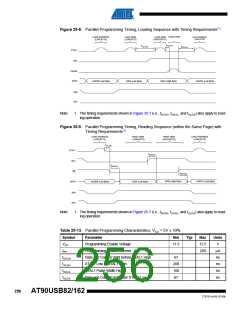
Depending on CKSEL Fuses, a valid clock must be present. The minimum low and high periods
for the serial clock (SCK) input are defined as follows:
Low: > 2 CPU clock cycles for fck < 12 MHz, 3 CPU clock cycles for fck >= 12 MHz
High: > 2 CPU clock cycles for fck < 12 MHz, 3 CPU clock cycles for fck >= 12 MHz
25.8.1
Serial Programming Algorithm
When writing serial data to the AT90USB82/162, data is clocked on the rising edge of SCK.
When reading data from the AT90USB82/162, data is clocked on the falling edge of SCK. See
Figure 25-11 for timing details.
To program and verify the AT90USB82/162 in the serial programming mode, the following
sequence is recommended (See four byte instruction formats in Table 25-16):
1. Power-up sequence:
Apply power between VCC and GND while RESET and SCK are set to “0”. In some sys-
tems, the programmer can not guarantee that SCK is held low during power-up. In this
case, RESET must be given a positive pulse of at least two CPU clock cycles duration
after SCK has been set to “0”.
2. Wait for at least 20 ms and enable serial programming by sending the Programming
Enable serial instruction to pin PDI.
3. The serial programming instructions will not work if the communication is out of syn-
chronization. When in sync. the second byte (0x53), will echo back when issuing the
third byte of the Programming Enable instruction. Whether the echo is correct or not, all
four bytes of the instruction must be transmitted. If the 0x53 did not echo back, give
RESET a positive pulse and issue a new Programming Enable command.
4. The Flash is programmed one page at a time. The memory page is loaded one byte at
a time by supplying the 7 LSB of the address and data together with the Load Program
258
AT90USB82/162
7707D–AVR–07/08

 ATMEL [ ATMEL ]