AT90USB82/162
19. USB controller
19.1 Features
• Support full-speed
• Support ping-pong mode (dual bank), with transparent switch
• 176 bytes of DPRAM
– 1 endpoint of 64 bytes max, (default control endpoint)
– 2 endpoints of 64 bytes max, (one bank)
– 2 endpoints of 64 bytes max, (one or two banks)
19.2 Block Diagram
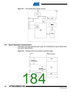
The USB controller provides the hardware to interface a USB link to a data flow stored in a dou-
ble port memory (DPRAM).
The USB controller requires a 48 MHz ±0.25% reference clock (for Full-speed compliance),
which is the output of an internal PLL. The PLL generates the internal high frequency (48 MHz)
clock for USB interface, the PLL input is generated from an external lower frequency (the crystal
oscillator or external clock input pin from XTAL1, to satisfy the USB frequency accuracy and jitter
; only this clock source allows proper functionnality of the USB controller).
The 48MHz clock is used to generate a 12 MHz Full-speed bit clock from the received USB dif-
ferential data and to transmit data according to full speed USB device tolerance. Clock recovery
is done by a Digital Phase Locked Loop (DPLL) block, which is compliant with the jitter specifica-
tion of the USB bus.
To comply the USB Electrical characteristics, USB Pads (D+ or D-) should be powered within
the 3.0 to 3.6V range. As AT90USB82/162 can be powered up to 5.5V, the internal regulator
provides the USB pads power supply.
183
7707D–AVR–07/08

 ATMEL [ ATMEL ]