27.7 AT90USB64/128 Boundary-scan Order
Table 27-3 shows the Scan order between TDI and TDO when the Boundary-scan chain is
selected as data path. Bit 0 is the LSB; the first bit scanned in, and the first bit scanned out. The
scan order follows the pin-out order as far as possible. Therefore, the bits of Port A and Port Fis
scanned in the opposite bit order of the other ports. Exceptions from the rules are the Scan
chains for the analog circuits, which constitute the most significant bits of the scan chain regard-
less of which physical pin they are connected to. In Figure 27-3, PXn. Data corresponds to FF0,
PXn. Control corresponds to FF1, PXn. Bit 4, 5, 6 and 7 of Port F is not in the scan chain, since
these pins constitute the TAP pins when the JTAG is enabled. The USB pads are not included in
the boundary-scan.
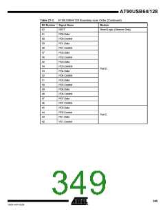
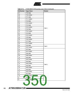
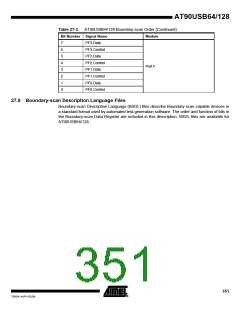
Table 27-3. AT90USB64/128 Boundary-scan Order
Bit Number Signal Name
Module
88
87
86
85
84
83
82
81
80
79
78
77
76
75
74
73
72
71
70
69
68
67
66
65
64
63
PE6.Data
PE6.Control
PE7.Data
Port E
PE7.Control
PE3.Data
PE3.Control
PB0.Data
PB0.Control
PB1.Data
PB1.Control
PB2.Data
PB2.Control
PB3.Data
PB3.Control
PB4.Data
Port B
PB4.Control
PB5.Data
PB5.Control
PB6.Data
PB6.Control
PB7.Data
PB7.Control
PE4.Data
PE4.Control
PE5.Data
PORTE
PE5.Control
348
AT90USB64/128
7593A–AVR–02/06

 ATMEL [ ATMEL ]