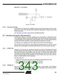
The active states are:
• Capture-DR: Data in the IDCODE Register is sampled into the Boundary-scan Chain.
• Shift-DR: The IDCODE scan chain is shifted by the TCK input.
27.4.3
SAMPLE_PRELOAD; 0x2
Mandatory JTAG instruction for pre-loading the output latches and taking a snap-shot of the
input/output pins without affecting the system operation. However, the output latches are not
connected to the pins. The Boundary-scan Chain is selected as Data Register.
The active states are:
• Capture-DR: Data on the external pins are sampled into the Boundary-scan Chain.
• Shift-DR: The Boundary-scan Chain is shifted by the TCK input.
• Update-DR: Data from the Boundary-scan chain is applied to the output latches. However,
the output latches are not connected to the pins.
27.4.4
AVR_RESET; 0xC
The AVR specific public JTAG instruction for forcing the AVR device into the Reset mode or
releasing the JTAG reset source. The TAP controller is not reset by this instruction. The one bit
Reset Register is selected as Data Register. Note that the reset will be active as long as there is
a logic “one” in the Reset Chain. The output from this chain is not latched.
The active states are:
• Shift-DR: The Reset Register is shifted by the TCK input.
27.4.5
BYPASS; 0xF
Mandatory JTAG instruction selecting the Bypass Register for Data Register.
The active states are:
• Capture-DR: Loads a logic “0” into the Bypass Register.
• Shift-DR: The Bypass Register cell between TDI and TDO is shifted.
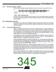
27.5 Boundary-scan Related Register in I/O Memory
27.5.1
MCU Control Register – MCUCR
The MCU Control Register contains control bits for general MCU functions.
Bit
7
6
–
R
0
5
–
R
0
4
3
–
R
0
2
–
R
0
1
0
JTD
R/W
0
PUD
R/W
0
IVSEL
R/W
0
IVCE
R/W
0
MCUCR
Read/Write
Initial Value
• Bits 7 – JTD: JTAG Interface Disable
When this bit is zero, the JTAG interface is enabled if the JTAGEN Fuse is programmed. If this
bit is one, the JTAG interface is disabled. In order to avoid unintentional disabling or enabling of
the JTAG interface, a timed sequence must be followed when changing this bit: The application
software must write this bit to the desired value twice within four cycles to change its value. Note
that this bit must not be altered when using the On-chip Debug system.
344
AT90USB64/128
7593A–AVR–02/06

 ATMEL [ ATMEL ]