AT90USB64/128
27.5.2
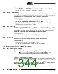
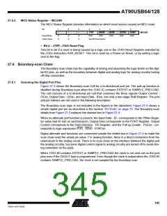
MCU Status Register – MCUSR
The MCU Status Register provides information on which reset source caused an MCU reset.
Bit
7
–
R
0
6
–
R
0
5
–
R
0
4
3
2
1
0
JTRF
R/W
WDRF
R/W
BORF
R/W
EXTRF
R/W
PORF
R/W
MCUSR
Read/Write
Initial Value
See Bit Description
• Bit 4 – JTRF: JTAG Reset Flag
This bit is set if a reset is being caused by a logic one in the JTAG Reset Register selected by
the JTAG instruction AVR_RESET. This bit is reset by a Power-on Reset, or by writing a logic
zero to the flag.
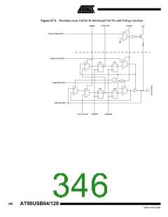
27.6 Boundary-scan Chain
The Boundary-scan chain has the capability of driving and observing the logic levels on the digi-
tal I/O pins, as well as the boundary between digital and analog logic for analog circuitry having
off-chip connection.
27.6.1
Scanning the Digital Port Pins
Figure 27-3 shows the Boundary-scan Cell for a bi-directional port pin. The pull-up function is
disabled during Boundary-scan when the JTAG IC contains EXTEST or SAMPLE_PRELOAD.
The cell consists of a bi-directional pin cell that combines the three signals Output Control -
OCxn, Output Data - ODxn, and Input Data - IDxn, into only a two-stage Shift Register. The port
and pin indexes are not used in the following description
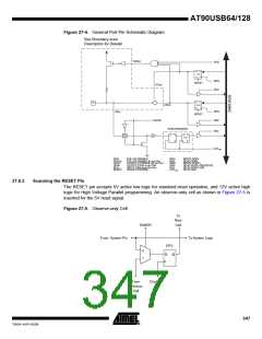
The Boundary-scan logic is not included in the figures in the datasheet. Figure 27-4 shows a
simple digital port pin as described in the section “I/O-Ports” on page 73. The Boundary-scan
details from Figure 27-3 replaces the dashed box in Figure 27-4.
When no alternate port function is present, the Input Data - ID - corresponds to the PINxn Regis-
ter value (but ID has no synchronizer), Output Data corresponds to the PORT Register, Output
Control corresponds to the Data Direction - DD Register, and the Pull-up Enable - PUExn - cor-
responds to logic expression PUD · DDxn · PORTxn.
Digital alternate port functions are connected outside the dotted box in Figure 27-4 to make the
scan chain read the actual pin value. For analog function, there is a direct connection from the
external pin to the analog circuit. There is no scan chain on the interface between the digital and
the analog circuitry, but some digital control signal to analog circuitry are turned off to avoid driv-
ing contention on the pads.
When JTAG IR contains EXTEST or SAMPLE_PRELOAD the clock is not sent out on the port
pins even if the CKOUT fuse is programmed. Even though the clock is output when the JTAG IR
contains SAMPLE_PRELOAD, the clock is not sampled by the boundary scan.
345
7593A–AVR–02/06

 ATMEL [ ATMEL ]