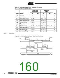
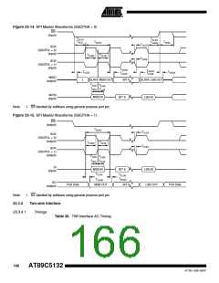
Table 112. External IDE 16-bit Bus Cycle – Data Read AC Timings
VDD = 2.7 to 3.3V, TA = -40° to +85°C
Variable Clock
Standard Mode
Variable Clock
X2 Mode
Symbol Parameter
Min
Max
Min
Max
Unit
ns
ns
ns
ns
ns
ns
ns
ns
ns
ns
ns
ns
ns
TCLCL
TLHLL
TAVLL
TLLAX
TLLRL
TRLRH
TRHLH
TAVDV
TAVRL
TRLDV
TRLAZ
TRHDX
TRHDZ
Clock Period
50
50
ALE Pulse Width
2·TCLCL-15
TCLCL-20
TCLCL-20
3·TCLCL-30
6·TCLCL-25
TCLCL-20
TCLCL-15
Address Valid to ALE Low
Address hold after ALE Low
ALE Low to RD Low
0.5·TCLCL-20
0.5·TCLCL-20
1.5·TCLCL-30
3·TCLCL-25
0.5·TCLCL-20
RD Pulse Width
RD high to ALE High
Address Valid to Valid Data In
Address Valid to RD Low
RD Low to Valid Data
RD Low to Address Float
Data Hold After RD High
Instruction Float After RD High
TCLCL+20
0.5·TCLCL+20
4.5·TCLCL-65
9·TCLCL-65
4·TCLCL-30
2·TCLCL-30
5·TCLCL-30
0
2.5·TCLCL-30
0
0
0
2·TCLCL-25
TCLCL-25
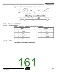
Table 113. External IDE 16-bit Bus Cycle – Data Write AC Timings
DD = 2.7 to 3.3V, TA = -40° to +85°C
V
Variable Clock
Standard Mode
Variable Clock
X2 Mode
Symbol Parameter
Min
Max
Min
50
Max
Unit
ns
ns
ns
ns
ns
ns
ns
ns
ns
ns
TCLCL
TLHLL
Clock Period
50
ALE Pulse Width
2·TCLCL-15
TCLCL-20
TCLCL-20
3·TCLCL-30
6·TCLCL-25
TCLCL-20
4·TCLCL-30
7·TCLCL-20
TCLCL-15
TCLCL-15
TAVLL
Address Valid to ALE Low
Address hold after ALE Low
ALE Low to WR Low
WR Pulse Width
0.5·TCLCL-20
0.5·TCLCL-20
1.5·TCLCL-30
3·TCLCL-25
TLLAX
TLLWL
TWLWH
TWHLH
TAVWL
TQVWH
TWHQX
WR High to ALE High
Address Valid to WR Low
Data Valid to WR High
Data Hold after WR High
TCLCL+20
0.5·TCLCL-20
2·TCLCL-30
0.5·TCLCL+20
3.5·TCLCL-20
0.5·TCLCL-15
162
AT89C5132
4173E–USB–09/07

 ATMEL [ ATMEL ]