AT85C51SND3Bx
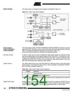
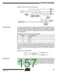
Figure 75. Audio DAC Interface Block Diagram
OCLK
DCLK
AUD
CLOCK
Clock Controller
0
DSEL
ADIEN
ADICON0.0
1
OVERS1:0 DSIZE
ADICON0.2:1 ADICON0.3
CSPOL
ADICON0.4
Data
DDAT
Converter
Audio Data From
Audio Processor
JUST4:0
ADICON1.4:0
Clock Controller
As soon as audio DAC interface is enabled by setting ADIEN bit in ADICON0, the mas-
ter clock generated by the clock generator (see Section “Clock Generator”) is output on
the OCLK pin which is the DAC over-sampling clock. The over-sampling ratio is defined
by OVERS1:0 bits in ADICON0 according to Table 164 and is selected depending on
the DAC capabilities.
Table 164. Audio DAC Interface Over-sampling Ratio
OVERS1:0
Over-sampling Ratio
Reserved
00
01
10
11
128 · FS
256 · FS
384 · FS
For DAC compatibility, the bit clock frequency is programmable for outputting 16 bits or
32 bits per channel using the DSIZE bit in ADICON0 (see Section "Data Converter",
page 157), and the word selection signal (DSEL) is programmable for outputting left
channel on low or high level according to CSPOL bit in ADICON0 as shown in
Figure 76.
Figure 76. DSEL Output Polarity
Left Channel
Left Channel
Right Channel
Right Channel
CSPOL = 0
CSPOL = 1
Data Converter
The data converter block converts the audio stream coming from the audio processor to
a serial format. For accepting all PCM formats and I2S format, JUST4:0 bits in ADICON1
register are used to shift the data output point. As shown in Figure 77, these bits allow
MSB justification by setting JUST4:0 = 00000, LSB justification by setting JUST4:0 =
10000, I2S Justification by setting JUST4:0 = 00001, and more than 16-bit LSB justifica-
tion by filling the low significant bits with logic 0.
157
7632A–MP3–03/06

 ATMEL [ ATMEL ]