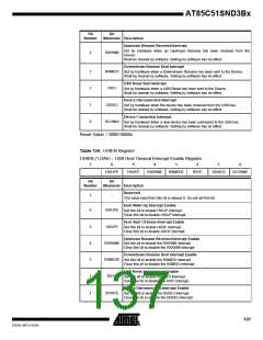
AT85C51SND3Bx
“Autoswitch” Mode
In this mode, the clear of the FIFOCON bit is performed automatically by hardware each
time the Pipe bank is full. The firmware has to check if the next bank is empty or not
before writing the next data. On TXOUT interrupt, the firmware fills a complete bank. A
new interrupt will be generated each time the current bank becomes free.
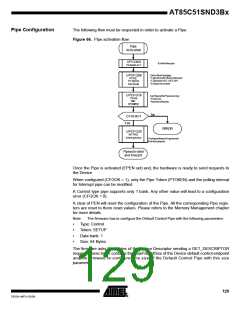
IN Pipe management
The Pipe must be configured first.
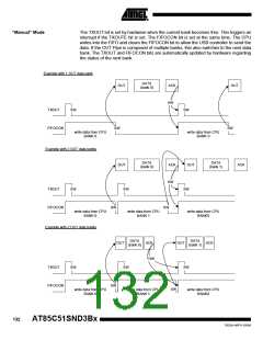
“Manual” Mode
When the Host requires data from the device, the firmware has to determine first the IN
mode to use using the INMODE bit:
•
INMODE = 0. The INRQX register is taken in account. The Host controller will
perform (INRQX+1) IN requests on the selected Pipe before freezing the Pipe. This
mode avoids to have extra IN requests on a Pipe.
•
INMODE = 1. The USB controller will perform infinite IN request until the firmware
freezes the Pipe.
The IN request generation will start when the firmware clear the PFREEZE bit.
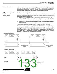
Each time the current bank is full, the RXIN and the FIFOCON bits are set. This triggers
an interrupt if the RXINE bit is set. The firmware can acknowledge the USB interrupt by
clearing the RXIN bit. The Firmware read the data and clear the FIFOCON bit in order to
free the current bank. If the IN Pipe is composed of multiple banks, clearing the FIFO-
CON bit will switch to the next bank. The RXIN and FIFOCON bits are then updated by
hardware in accordance with the status of the new bank.
Example with 1 IN data bank
DATA
(to bank 0)
DATA
(to bank 0)
IN
ACK
HW
IN
ACK
HW
RXIN
SW
SW
FIFOCON
SW
read data from CPU
BANK 0
read data from CPU
BANK 0
Example with 2 IN data banks
DATA
(to bank 0)
DATA
(to bank 1)
IN
ACK
HW
IN
ACK
HW
RXIN
SW
SW
FIFOCON
SW
read data from CPU
BANK 0
read data from CPU
BANK 1
133
7632A–MP3–03/06

 ATMEL [ ATMEL ]