Instruction Set
TSC695F instructions fall into six functional categories: load/store, arithmetic/logi-
cal/shift, control transfer, read/write control register, floating-point, and miscellaneous.
Please refer to SPARC V7 Instruction-set Manual.
Note:
The execution of IFLUSH will cause an illegal instruction trap.
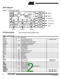
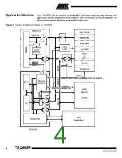
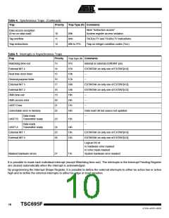
On-chip Peripherals
Memory Interface
The TSC695F is designed to allow easy interfacing to internal/external memory
resources.
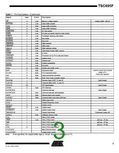
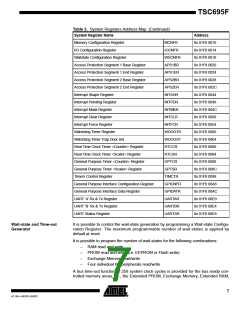
Table 2. Memory Mapping
Memory Contents
Start Address
Size (bytes)
Data Size and Parity Options
Boot PROM
0x00000000
0x01000000
128K → 16M
8-bit mode
40-bit mode
8-bit mode
40-bit mode
No parity/-No EDAC/-Only byte write
Parity + EDAC mandatory/-Only word write
No parity/-No EDAC/-Only byte write
Extended PROM
Max: 15M
Parity + EDAC mandatory/-Only word write
Exchange Memory
System Registers
RAM (8 blocks)
Extended RAM
I/O Area 0
0x01F00000
0x01F80000
0x02000000
0x04000000
0x10000000
0x11000000
0x12000000
0x13000000
0x14000000
0x80000000
4k → 512k
512K (124 used)
8*32K → 8*4M
Max: 192M
0 → 16M
Parity + EDAC option/-Only word write
Parity/-Only word read/write access
Parity + EDAC option/-All data sizes allowed
Parity option/-All data sizes allowed
I/O Area 1
0 → 16M
I/O Area 2
0 → 16M
I/O Area 3
0 → 16M
Extended I/O Area
Extended General
Max: 1728M
Max: 2G
No parity/-All data sizes allowed
System Registers
The system registers are only writable by IU in the supervisor mode or by DMA during
halt mode.
Table 3. System Registers Address Map
System Register Name
System Control Register
Software Reset
Address
SYSCTR
SWRST
PDOWN
SYSFSR
FAILAR
0x 01F8 0000
0x 01F8 0004
0x 01F8 0008
0x 01F8 00A0
0x 01F8 00A4
0x 01F8 00B0
0x 01F8 00D0
Power Down
System Fault Status Register
Failing Address Register
Error & Reset Status Register
Test Control Register
ERRRSR
TESCTR
6
TSC695F
4118H–AERO–06/03

 ATMEL [ ATMEL ]