Extended I/O and the Extended General areas.
EDAC
The TSC695F includes a 32-bit EDAC (Error Detection And Correction). Seven bits
(CB[6:0]) are used as check bits over the data bus. The Data Bus Parity signal (DPAR)
is used to check and generate the odd parity over the 32-bit data bus. This means that
altogether 40 bits are used when the EDAC is enabled.
The TSC695F EDAC uses a 7-bit Hamming code which detects any double bit error on
the 40-bit bus as a non-correctable error. In addition, the EDAC detects all bits stuck-at-
one and stuck-at-zero failure for any nibble in the data word as a non-correctable error.
Stuck-at-one and stuck-at-zero for all 32 bits of the data word is also detected as a non-
correctable error.
Memory and I/O Parity
The TSC695F handles parity towards memory and I/O in a special way. The processor
can be programmed to use no parity, only parity or parity and EDAC protection towards
memory and to use parity or no towards I/O. The signal used for the parity bit is DPAR.
Memory Redundancy
Programming the Memory Configuration Register, the TSC695F provides chip selects
for two redundant memory banks for replacement of faulty banks.
Memory Access Protection
•
•
Unimplemented Areas - Access to all unimplemented memory areas are handled by
the TSC695F and detected as illegal.
RAM Write Access Protection - The TSC695F can be programmed to detect and
mask write accesses in any part of the RAM. The protection scheme is enabled only
for data area, not for the instruction area. The programmable write access
protection is based on two segments.
•
Boot PROM Write Protection - The TSC695F supports a qualified PROM write for
an 8-bit wide PROM and/or for a 40-bit wide PROM.
DMA
DMA Interface
The TSC695F supports Direct Memory Access (DMA). The DMA unit requests access
to the processor bus by asserting the DMA request signal (DMAREQ). When the DMA
unit receives the DMAGNT signal in response, the processor bus is granted. In case the
processor is in the power-down mode the processor is permanent tri-stated, and a
DMAREQ will directly give a DMAGNT. The TSC695F includes a DMA session time-out
function.
Bus Arbiter
The TSC695F always has the lowest priority on the system bus.
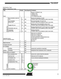
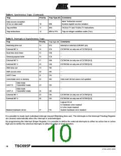
Traps
A trap is a vectored transfer of control to the supervisor through a special trap table that
contains the first four instructions of each trap handler. The base address of the table is
established by supervisor and the displacement, within the table, is determined by the
trap type. Two categories of traps can appear.
8
TSC695F
4118H–AERO–06/03

 ATMEL [ ATMEL ]