Torwards
AT8563
AT8563’s pin layout and its protection network are shown in Fig 2 and Fig 3.
Fig 3 Device diode protection diagram
Fig 2 Pin Layout
Table 3 gives the pins’ description.
Table 3: Pin description
Description
Symbol
OSCI
OSCO
INT
Pin
1
oscillator input
oscillator output
2
3
interrupt output (open-drain; active LOW)
ground
VSS
4
SDA
5
serial Data I/O (open-drain)
serial Clock in
SCL
6
CLKOUT
VDD
7
clock output (open-drain)
positive power supply
8
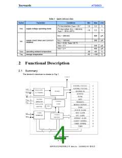
AT8563 contains sixteen 8-bit registers with an auto-increasing address register, an
on-chip 32.768 kHz oscillator with an integrated capacitor, a frequency divider which provides
source clock for the Real-Time Clock (RTC), a programmable clock output, a timer, an alarm, a
voltage-low detector and a I2C-bus interface.
The 16 registers are mapped into a memory block, which is addressable, but not all bits
are implemented. The first two registers (memory address 00H and 01H) are used as control
and/or status registers. The memory addresses 02H through 08H are used as counters for the
clock function (seconds up to year counters). Address locations 09H through 0CH contain
alarm registers which define the conditions for an alarm. Address 0DH controls the frequency
of CLKOUT output. 0EH and 0FH are timer control, timer counter register, respectively.
The Seconds, Minutes, Hours, Days, Months, Years as well as the Minute alarm, Hour
alarm and Day alarm registers are all coded in BCD format. The Weekdays and Weekday
alarm register are not coded in BCD format.
When one of the RTC registers is read the contents of all counters are frozen. Therefore,
•
3
•
深圳市宏达科技有限公司 Mobile:13530382140 曾先生

 Narda-ATM [ Narda-ATM ]