AOZ1284
Combination of R1 and R2 should be large enough to
avoid drawing excessive current from the output,
which will cause power loss.
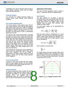
Application Information
The basic AOZ1284 application circuit is shown in
Figure 1. Component selection is explained below.
Protection Features
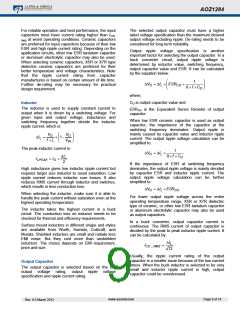
Input capacitor
The AOZ1284 has multiple protection features to
prevent system circuit damage under abnormal
conditions.
The input capacitor (C1 in Figure 1) must be
connected to the VIN pin and GND pin of the AOZ1284
to maintain steady input voltage and filter out the
pulsing input current. The voltage rating of input
capacitor must be greater than maximum input
voltage plus ripple voltage.
Over Current Protection (OCP)
The sensed inductor current signal is also used for
over current protection. Since the AOZ1284 employs
peak current mode control, the COMP pin voltage is
proportional to the peak inductor current. The COMP
pin voltage is limited to be between 0.4V and 2.5V
internally. The peak inductor current is automatically
limited cycle by cycle.
The input ripple voltage can be approximated by
equation below:
IO
VO
VO
VI
1
N
f CI
VI
VI
N
N
N
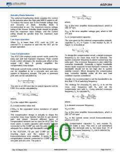
Since the input current is discontinuous in a buck
converter, the current stress on the input capacitor is
another concern when selecting the capacitor. For a
buck circuit, the RMS value of input capacitor current
can be calculated by:
The cycle by cycle current limit threshold is internally
set. When the load current reaches the current limit
threshold, the cycle by cycle current limit circuit turns
off the high side switch immediately to terminate the
current duty cycle. The inductor current stop rising.
The cycle by cycle current limit protection directly
limits inductor peak current. The average inductor
current is also limited due to the limitation on peak
inductor current. When cycle by cycle current limit
circuit is triggered, the output voltage drops as the
duty cycle decreasing.
V
V
O
O
I
I
1
CIN _RMS
O
V
V
IN
IN
if let m equal the conversion ratio:
VO
m
VIN
The AOZ1284 has internal short circuit protection to
protect itself from catastrophic failure under output
short circuit conditions. The FB pin voltage is
proportional to the output voltage. Whenever FB pin
voltage is below 0.2V, the short circuit protection
circuit is triggered.
The relation between the input capacitor RMS current
and voltage conversion ratio is calculated and shown
below in Figure 2. It can be seen that when VO is half
of VIN, CIN is under the worst current stress. The worst
current stress on CIN is 0.5·IO.
Power-On Reset (POR)
0.5
0.5
A power-on reset circuit monitors the input voltage.
When the input voltage exceeds 2.9V, the converter
starts operation. When input voltage falls below 2.3V,
the converter will stop switching.
0.4
0.3
I
(m)
CIN_RMS
I
O
0.2
0.1
0
Thermal Protection
An internal temperature sensor monitors the junction
temperature. It shuts down the internal control circuit
and high side NMOS if the junction temperature
exceeds 145ºC. The regulator will restart
automatically under the control of soft-start circuit
when the junction temperature decreases to 100ºC.
0
0
0.5
m
1
0
1
Figure 2. ICIN vs. Voltage conversion ratio
www.aosmd.com
Page 8 of 14
Rev. 0.5 March 2012

 AOS [ ALPHA & OMEGA SEMICONDUCTORS ]