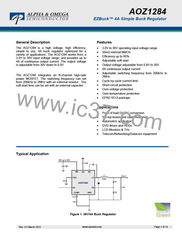
AOZ1284
Schottky Diode Selection
G
EA
f
P2
The external freewheeling diode supplies the current
to the inductor when the high side NMOS switch is off.
To reduce the losses due to the forward voltage drop
and recovery of diode, Schottky diode is
recommended to use. The maximum reverse voltage
rating of the chosen Schottky diode should be greater
than the maximum input voltage, and the current
rating should be greater than the maximum load
current.
2 C G
C
VEA
where;
GEA is the error amplifier transconductance, which is
200·10-6 A/V;
GVEA is the error amplifier voltage gain, which is 500
V/V and
CC is compensation capacitor.
Low Input operation
The zero given by the external compensation network,
capacitor CC (C5 in Figure 1) and resistor RC (R1 in
Figure 1), is located at:
When VIN is lower than 4.5V, such as 3.0V, an
external 5V is required to add into the BST pin for
proper operation.
1
f
Z2
2 C R
C
C
Loop Compensation
To design the compensation circuit, a target crossover
frequency fC for close loop must be selected. The
system crossover frequency is where control loop has
unity gain. The crossover frequency is also called the
converter bandwidth. Generally a higher bandwidth
means faster response to load transient. However, the
bandwidth should not be too high due to system
stability concern. When designing the compensation
loop, converter stability under all line and load
condition must be considered.
The AOZ1284 employs peak current mode control for
easy use and fast transient response. Peak current
mode control eliminates the double pole effect of the
output L&C filter. It greatly simplifies the
compensation loop design.
With peak current mode control, the buck power stage
can be simplified to be a one-pole and one-zero
system in frequency domain. The pole is dominant
pole and can be calculated by:
Usually, it is recommended to set the bandwidth to be
less than 1/10 of switching frequency.
1
f
P1
2 C R
O
L
The strategy for choosing RC and CC is to set the
cross over frequency with RC and set the
compensator zero with CC. Using selected crossover
frequency, fC, to calculate RC:
The zero is a ESR zero due to output capacitor and its
ESR. It is can be calculated by:
1
f
Z1
2 C ESR
V
2 C
O
O
CO
O
R
f
C
C
V
G
G
FB
EA CS
where;
where;
fC is desired crossover frequency;
FB is 0.8V;
CO is the output filter capacitor;
RL is load resistor value and
V
ESRCO is the equivalent series resistance of output
capacitor.
GEA is the error amplifier transconductance, which is
200·10-6 A/V and
The compensation design is actually to shape the
converter close loop transfer function to get desired
gain and phase. Several different types of
compensation network can be used for AOZ1284. For
most cases, a series capacitor and resistor network
connected to the COMP pin sets the pole-zero and is
adequate for a stable high-bandwidth control loop.
GCS is the current sense circuit transconductance,
which is 4.5 A/V.
The compensation capacitor CC and resistor RC
together make a zero. This zero is put somewhere
close to the dominate pole fp1 but lower than 1/5 of
selected crossover frequency. CC can is selected by:
In the AOZ1284, FB pin and COMP pin are the
inverting input and the output of internal
transconductance error amplifier. A series R and C
compensation network connected to COMP provides
one pole and one zero. The pole is:
1.5
C
C
2 R f
C
P1
www.aosmd.com
Page 10 of 14
Rev. 0.5 March 2012

 AOS [ ALPHA & OMEGA SEMICONDUCTORS ]