AOZ1284
COMP pin, is compared against the current signal,
which is sum of inductor current signal and ramp
compensation signal, at PWM comparator input. If the
current signal is less than the error voltage, the
internal high-side switch is on. The inductor current
flows from the input through the inductor to the output.
When the current signal exceeds the error voltage, the
high-side switch is off. The inductor current is
freewheeling through the Schottky diode to output.
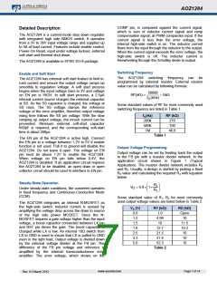
Detailed Description
The AOZ1284 is a current-mode step down regulator
with integrated high side NMOS switch. It operates
from a 3V to 36V input voltage range and supplies up
to 4A of load current. Features include enable control,
Power-On Reset, input under voltage lockout, external
soft-start and thermal shut down.
The AOZ1284 is available in EPAD SO-8 package.
Switching Frequency
Enable and Soft Start
The AOZ1284 switching frequency can be
programmed by external resistor. External resistor
value can be calculated by following formula.
The AOZ1284 has external soft start feature to limit in-
rush current and ensure the output voltage ramps up
smoothly to regulation voltage. A soft start process
begins when the input voltage rises to 3V and voltage
on EN pin is HIGH. In soft start process, a 2.5µA
internal current source charges the external capacitor
at SS. As the SS capacitor is charged, the voltage at
SS rises. The SS voltage clamps the reference
voltage of the error amplifier, therefore output voltage
rising time follows the SS pin voltage. With the slow
ramping up output voltage, the inrush current can be
prevented. Minimum external soft-start capacitor
850pF is required, and the corresponding soft-start
time is about 200µs.
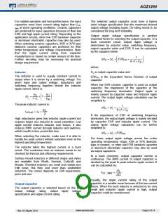
50000
RF(k)
5k
f (kHz)
O
Some standard values of RF for most commonly used
switching frequency are listed in Table 1.
fO(Hz)
200k
500k
1M
RF (kΩ)
270
100
46.6
Table 1
The EN pin of the AOZ1284 is active high. Connect
the EN pin to a voltage between 1.2V to 5V if enable
function is not used. Pull it to ground will disable the
AOZ1284. Do not leave it open. The voltage on EN
pin must be above 1.2V to enable the AOZ1284.
When voltage on EN pin falls below 0.4V, the
AOZ1284 is disabled. If an application circuit requires
the AOZ1284 to be disabled, an open drain or open
collector circuit should be used to interface to EN pin.
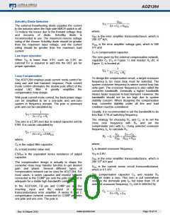
Output Voltage Programming
Output voltage can be set by feeding back the output
to the FB pin with a resistor divider network. In the
application circuit shown in Figure
Application). The resistor divider network includes R2
and R3. Usually, a design is started by picking a fixed
R3 value and calculating the required R2 with equation
below.
1
(Typical
Steady-State Operation
R
1
V
0.8 1
O
Under steady-state conditions, the converter operates
in fixed frequency and Continuous-Conduction Mode
(CCM).
R
2
Some standard value of R1, R2 for most commonly
used output voltage values are listed below in Table 2.
The AOZ1284 integrates an internal N-MOSFET as
the high-side switch. Inductor current is sensed by
amplifying the voltage drop across the drain to source
of the high side power MOSFET. Since the N-
MOSFET requires a gate voltage higher than the input
voltage, a boost capacitor connected between LX pin
and BST pin drives the gate. The boost capacitor is
charged while LX is low. An internal 10Ω switch from
LX to GND is used to insure that LX is pulled to GND
even in the light load. Output voltage is divided down
by the external voltage divider at the FB pin. The
difference of the FB pin voltage and reference is
amplified by the internal transconductance error
amplifier. The error voltage, which shows on the
VO (V)
0.8
R1 (kΩ)
1.0
R2 (kΩ)
Open
10
1.2
4.99
10
1.5
11.5
10.2
10
1.8
12.7
21.5
31.6
52.3
Table 2
2.5
3.3
10
5.0
10
www.aosmd.com
Page 7 of 14
Rev. 0.5 March 2012

 AOS [ ALPHA & OMEGA SEMICONDUCTORS ]