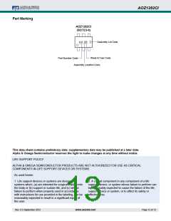
AOZ1282CI
When selecting the inductor, make sure it is able to
handle the peak current without saturation even at the
highest operating temperature.
For lower output ripple voltage across the entire
operating temperature range, X5R or X7R dielectric type
of ceramic, or other low ESR tantalum capacitor or
aluminum electrolytic capacitor may also be used as
output capacitors.
The inductor takes the highest current in a buck circuit.
The conduction loss on inductor needs to be checked for
thermal and efficiency requirements.
In a buck converter, output capacitor current is
continuous. The RMS current of output capacitor is
decided by the peak to peak inductor ripple current.
It can be calculated by:
Surface mount inductors in different shape and styles are
available from Coilcraft, Elytone and Murata. Shielded
inductors are small and radiate less EMI noise. But they
cost more than unshielded inductors. The choice
depends on EMI requirement, price and size.
I
L
----------
I
=
CO_RMS
12
Output Capacitor
Usually, the ripple current rating of the output capacitor is
a smaller issue because of the low current stress. When
the buck inductor is selected to be very small and
inductor ripple current is high, output capacitor could be
overstressed.
The output capacitor is selected based on the DC output
voltage rating, output ripple voltage specification and
ripple current rating.
The selected output capacitor must have a higher rated
voltage specification than the maximum desired output
voltage including ripple. De-rating needs to be
considered for long term reliability.
Schottky Diode Selection
The external freewheeling diode supplies the current to
the inductor when the high side NMOS switch is off. To
reduce the losses due to the forward voltage drop and
recovery of diode, Schottky diode is recommended to
use. The maximum reverse voltage rating of the chosen
Schottky diode should be greater than the maximum
input voltage, and the current rating should be greater
than the maximum load current.
Output ripple voltage specification is another important
factor for selecting the output capacitor. In a buck
converter circuit, output ripple voltage is determined by
inductor value, switching frequency, output capacitor
value and ESR. It can be calculated by the equation
below:
1
Thermal Management and Layout
Consideration
-------------------------
V = I ESR
+
O
L
CO
8 f C
O
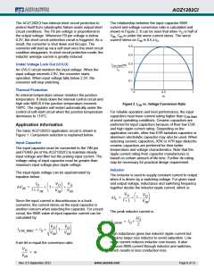
In the AOZ1282CI buck regulator circuit, high pulsing
current flows through two circuit loops. The first loop
starts from the input capacitors, to the VIN pin, to the LX
pins, to the filter inductor, to the output capacitor and
load, and then return to the input capacitor through
ground. Current flows in the first loop when the high side
switch is on. The second loop starts from inductor, to the
output capacitors and load, to the anode of Schottky
diode, to the cathode of Schottky diode. Current flows in
the second loop when the low side diode is on.
where,
C is output capacitor value, and
O
ESR is the equivalent series resistance of the output
CO
capacitor.
When low ESR ceramic capacitor is used as output
capacitor, the impedance of the capacitor at the switching
frequency dominates. Output ripple is mainly caused by
capacitor value and inductor ripple current. The output
ripple voltage calculation can be simplified to:
In PCB layout, minimizing the two loops area reduces the
noise of this circuit and improves efficiency. A ground
plane is strongly recommended to connect input
capacitor, output capacitor, and PGND pin of the
AOZ1282CI.
1
-------------------------
V = I
O
L
8 f C
O
If the impedance of ESR at switching frequency
dominates, the output ripple voltage is mainly decided by
capacitor ESR and inductor ripple current. The output
ripple voltage calculation can be further simplified to:
In the AOZ1282CI buck regulator circuit, the major power
dissipating components are the AOZ1282CI, the
Schottky diode and output inductor. The total power
dissipation of converter circuit can be measured by input
power minus output power.
V = I ESR
CO
O
L
P
= V I – V V
IN IN O IN
total_loss
www.aosmd.com
Rev. 0.5 September 2012
Page 9 of 13

 AOS [ ALPHA & OMEGA SEMICONDUCTORS ]