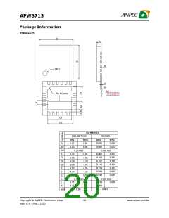
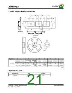
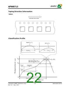
APW8713
Application Information (Cont.)
Input Capacitor Selection
Layout Consideration
The input capacitor is chosen based on the voltage rating
and the RMS current rating. For reliable operation, select-
ing the capacitor voltage rating to be at least 1.3 times
higher than the maximum input voltage. The maximum
RMS current rating requirement is approximately IOUT/2,
where IOUT is the load current. During power-up, the input
capacitors have to handle great amount of surge current.
For low-duty notebook applications, ceramic capacitor is
recommended. The capacitors must be connected be-
tween the drain of high-side MOSFET and the source of
low-side MOSFET with very low-impedance PCB layout.
In any high switching frequency converter, a correct lay-
out is important to ensure proper operation of the
regulator. With power devices switching at higher
frequency, the resulting current transient will cause volt-
age spike across the interconnecting impedance and
parasitic circuit elements. As an example, consider the
turn-off transition of the PWM MOSFET. Before turn-off
condition, the MOSFET is carrying the full load current.
During turn-off, current stops flowing in the MOSFET and
is freewheeling by the low side MOSFET and parasitic
diode. Any parasitic inductance of the circuit generates a
large voltage spike during the switching interval. In
general, using short and wide printed circuit traces should
minimize interconnecting impedances and the magni-
tude of voltage spike. Besides, signal and power grounds
are to be kept separate and finally combined using ground
plane construction or single point grounding. The best
tie-point between the signal ground and the power ground
is at the negative side of the output capacitor on each
channel, where there is less noise. Noisy traces beneath
the IC are not recommended. Below is a checklist for
your layout:
Thermal Consideration
Because the APW8802 build-in high-side and low-side
MOSFET, the heat dissipated may exceed the maximum
junction temperature of the part in applications. If the junc-
tion temperature reaches approximately 150oC, both
power switches will be turned off and the LX node will
become high impedance. To avoid the APW8713 from
exceeding the maximum junction temperature, the user
will need to do some thermal analysis. The goal of the
thermal analysis is to determine whether the power dis-
sipated exceeds the maximum junction temperature of
the part. The main power dissipated by the part is
approximated:
- Keep the switching nodes (BOOT and LX) away from
sensitive small signal nodes since these nodes are
fast moving signals. Therefore, keep traces to these
nodes as short as possible and there should be no
other weak signal traces in parallel with theses traces
on any layer.
PUPPER = IO2 UT(1+ TC)(RDS(ON))D + 0.5(IOUT)(V )(tSW )FSW
IN
= IO2 UT(1+ TC)(RDS(ON))(1-D)
- The large layout plane between the drain of the MOSFETs
(VIN and LX nodes) can get better heat sinking.
- The current sense resistor should be close to OCSET
pin to avoid parasitic capacitor effect and noise coupling.
- Decoupling capacitors, the resistor-divider, and boot
capacitor should be close to their pins.
P
LOWER
IOUT is the load current
TC is the temperature dependency of RDS(ON)
FSW is the switching frequency
tSW is the switching interval
- The output bulk capacitors should be close to the loads.
The input capacitor’s ground should be close to the
grounds of the output capacitors.
D is the duty cycle
Note that both internal MOSFETs have conduction losses
while the upper MOSFET include an additional transition
loss. The switching internal, tSW, is the function of the
reverse transfer capacitance CRSS. The (1+TC) term fac-
tors in the temperature dependency of the RDS(ON) and can
be extracted from the "RDS(ON) vs. Temperature" curve
of the power MOSFET. In APW8713 case, the RDS(ON) is
about 30mW from specification table.
- Locate the resistor-divider close to the FB pin to mini-
mize the high impedance trace. In addition, FB pin traces
can’t be close to the switching signal traces (BOOT and
LX).
Copyright ã ANPEC Electronics Corp.
18
www.anpec.com.tw
Rev. A.3 - Sep., 2013

 ANPEC [ ANPEC ELECTRONICS COROPRATION ]