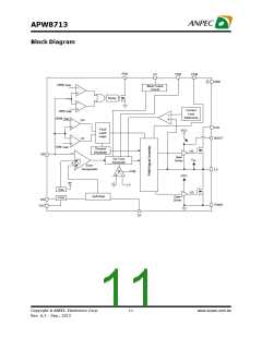
APW8713
Function Description (Cont.)
Soft-Start
Under-Voltage Protection (UVP)
The APW8713 provides the programmed soft-start func-
tion to limit the inrush current. The soft-start time can be
programmed by the external capacitor between SS and
GND. Typical charge current is 10uA, and the soft-start
time can be calculated by the following formula:
In the process of operation, if a short circuit occurs, the
output voltage will drop quickly. When load current is big-
ger than current limit threshold value, the output voltage
will fall out of the required regulation range. The under-
voltage protection circuit continually monitors the FB volt-
age after soft-start is completed. If a load step is strong
enough to pull the output voltage lower than the under
voltage threshold, the under voltage threshold is 70% of
the nominal output voltage, the internal UVP delay counter
starts to count. After 16ms de-bounce time, the device
turns off both high side and low-side MOSEFET with
latched. Toggling enable pin to low, or recycling VIN, will
clear the latch and bring the chip back to operation.
TSS(ms) = 330´ CSS(nF)
The APW8713 integrates soft-start circuits to ramp up the
output voltage of the converter to the programmed regu-
lation set point at a predictable slew rate. The slew
rate of output voltage is internally controlled to limit the
inrush current through the output capacitors during soft-
start process. When the EN pin is pulled above the rising
EN threshold voltage, the device initiates a soft-start pro-
cess to ramp up the output voltage.
Over-Voltage Protection (OVP)
The over voltage function monitors the output voltage by
FB pin. Should the FB voltage increase over 125% of the
reference voltage due to the high-side MOSFET failure or
for other reasons, the over voltage protection comparator
designed with a 3ms noise filter will force the low-side
MOSFET gate driver fully turn on and latch high. This ac-
tion actively pulls down the output voltage.
During soft-start stage before the PGOOD pin is ready,
the under voltage protection is prohibited. The over volt-
age and current limit protection functions are enabled. If
the output capacitor has residue voltage before startup,
both low-side and high-side MOSFETs are in off-state
until the soft start voltage equal the VFB voltage. This will
ensure the output voltage starts from its existing voltage
level.
This OVP scheme only clamps the voltage overshoot,
and does not invert the output voltage when otherwise
activated with a continuously high output from low-side
MOSFET driver. It’s a common problem for OVP schemes
with a latch. Once an over-voltage fault condition is set, it
can only be reset by toggling EN or VIN power-on-reset
signal.
In the event of under-voltage, over-voltage, over-tempera-
ture or shutdown, the chip enables the soft-stop function.
The soft-stop function discharges the output voltages by
low side turns MOSFET on linearly.
Power Good Indicator
POK is actively held low in shutdown and soft-start status.
In the soft-start process, the POK is an open-drain. When
the soft-start is finished, the POK is released. In normal
operation, the POK window is from 90% to 125% of the
converter reference voltage. When the output voltage has
to stay within this window, POK signal will become high.
When the output voltage outruns 90% or 125% of the
target voltage, POK signal will be pulled low immediately.
In order to prevent false POK drop, capacitors need to
parallel at the output to confine the voltage deviation with
severe load step transient.
Current Limit
The current limit circuit employs a "valley" current-sens-
ing algorithm (See Figure 1). The APW8713 uses the
low-side MOSFET’s RDS(ON) of the synchronous rectifier
as a current-sensing element. If the magnitude of the
current-sense signal at LX pin is above the current-limit
threshold 11A(minimum), the PWM is not allowed to ini-
tiate a new cycle. The actual peak current is greater than
the current-limit threshold by an amount equal to the in-
ductor ripple current. Therefore, the exact current-limit char-
acteristic and maximum load capability are a function of
the sense resistance, inductor value, and input voltage.
Copyright ã ANPEC Electronics Corp.
15
www.anpec.com.tw
Rev. A.3 - Sep., 2013

 ANPEC [ ANPEC ELECTRONICS COROPRATION ]