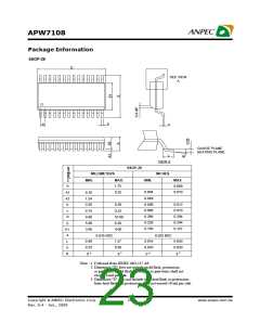
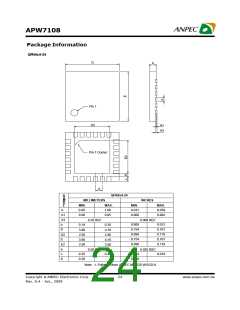
APW7108
Application Information (Cont.)
conduction loss and transition loss. For the high-side
and low-side MOSFETs, the losses are approximately
given by the following equations:
Input Capacitor Selection
select the capacitor voltage rating to be at least 1.3 times
higher than the maximum input voltage. The maximum
RMS current rating requirement is approximately IOUT/2,
where IOUT is the load current. During power up, the
input capacitors have to handle large amount of surge
current. In low-duty notebook appliactions, ceramic ca-
pacitors are recommended. The capacitors must be con-
nected between the drain of high-side MOSFET and the
source of low-side MOSFET with very low-impeadance
PCB layout.
Phigh-side = IOUT 2(1+ TC)(RDS(ON))D + (0.5)( IOUT)(V )( tSW)FSW
IN
Plow-side = IOUT 2(1+ TC)(RDS(ON))(1-D)
Where
I
is the load current
OUT
TC is the temperature dependency of RDS(ON)
FSW is the switching frequency
tSW is the switching interval
D is the duty cycle
MOSFETSelection
Note that both MOSFETs have conduction losses while
the high-side MOSFET includes an additional tran-
sition loss. The switching internal, tSW, is the func-
tion of the reverse transfer capacitance CRSS. The (1+TC)
term is to factor in the temperature dependency of the RDS
The application for a notebook battery with a maximum volt-
age of 24V, at least a minimum 30V MOSFETs should
be used. The design has to trade off the gate charge with
the RDS(ON) of the MOSFET:
and can be extracted from the “R DS(ON) vs Tempera-
(ON)
·
For the low-side MOSFET, before it is turned on, the
bodydiode has been conducted. The low-side MOSFET
driver will not charge the miller capacitor of this
MOSFET.
ture” curve of the power MOSFET.
Layout Consideration
In any high switching frequency converter, a correct layout
is important to ensure proper operation of the regulator.
With power devices switching at higher frequency, the
resulting current transient will cause voltage spike across
the interconnecting impedance and parasitic circuit
elements. As an example, consider the turn-off transition
of the PWM MOSFET. Before turn-off condition, the
MOSFET is carrying the full load current. During turn-off,
current stops flowing in the MOSFET and is freewheeling
by the low-side MOSFET and parasitic diode. Any para-
sitic inductance of the circuit generates a large voltage
spike during the switching interval. In general, using short
and wide printed circuit traces should minimize intercon-
necting impedances and the magnitude of voltage spike.
Signal and power grounds are to be kept separating and
finally combined using ground plane construction or
single point grounding. The best tie-point between the
signal ground and the power ground is at the negative
side of the output capacitor on each channel, where there
is less noise. Noisy traces beneath the IC are not
recommended. Below is a checklist for your layout:
·
In the turning-off process of the low-side MOSFET,
the load current will shift to the body diode first. The
high dv/dt of the phase node voltage will charge the
miller capacitor through the low-side MOSFET driver
sinking current path. This results in much less
switching loss of the low-side MOSFETs.The duty
cycle is often very small in high battery voltage
applications, and the low-side MOSFET will con-
duct most of the switching cycle; therefore, the less
the RDS(ON) of the low-side MOSFET loss, the less the
power loss. The gate charge for this MOSFET is usu-
ally of secondary consideration. The high-side
MOSFET does not have the zero voltage switch-
ing condition, and because it conducts for less time
compared to the low-side MOSFET, the switching
loss tends to be dominant. Priority should be given
to the MOSFETs with less gate charge, so that both
the gate driver loss and switching loss will be
minimized.
The selection of the N-channel power MOSFETs are
determined by the RDS(ON), reversing transfer capaci-
tance (CRSS) and maximum output current requirement.
The losses in the MOSFETs have two components:
Copyright ã ANPEC Electronics Corp.
21
www.anpec.com.tw
Rev. A.4 - Jan., 2009

 ANPEC [ ANPEC ELECTRONICS COROPRATION ]