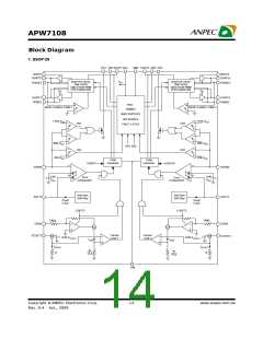
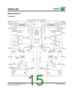
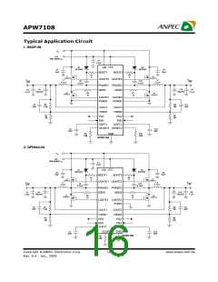
APW7108
Function Description (Cont.)
ing as a sinking linear regulator. The soft-stop process is
completed when the falling SOFT voltage reaches about
50mV (typical) threshold. At this moment, the LGATE goes
high level with latch and SOFT pulls low by using the
internal 2kW resistor to the ground. The latch can be re-
set by cycling both of the EN signals or VCC power-on-
reset signal.
Power-On-Reset
set high. When the rising VCC voltage reaches the ris-
ing POR voltage threshold (4.2V typical), the POR sig-
nal goes high and the chip initiates soft-start opera-
tions for the enabled channels. This voltage should
drop lower than 4V (typical), the POR disables the chip.
Soft-Start/Soft-Stop
Under-Voltage Protection (UVP)
When soft-start is initiated, the voltage on the SOFT pin of
the enabled channel starts to ramp up gradually with the
internal 4.5mA current charging the soft-start capacitor. The
output voltage follows the soft-start voltage with the
converter operating in PWM mode. When the SOFT pin
voltage reaches 0.9V, the output voltage comes into
regulation. When the SOFT voltage reaches 1.5V, the
power-good (PGOOD) is enabled. Even though the SOFT
pin voltage continues to rise after reaching 1.5V, this
voltage does not affect the output voltage. The maxi-
mum SOFT voltage is clamped about 2.4V.
In the operational process, if a short-circuit occurs, the
output voltage will drop quickly. When load current is bigger
than current-limit threshold value, the output voltage will
fall out of the required regulation range. The under-
voltage continually monitors the VSEN voltage after soft-
start is completed. If a load step is strong enough to pull
the output voltage lower than the under-voltage
threshold, the offending channel pulls low the PGOOD
immediately and starts a soft-stop process to shut down
the output gradually. The offending channel is latched
off when the soft-stop process is completed.
The soft-start time (the time from the moment when EN
becomes high to the moment when PGOOD is reported)
is determined by the following equation:
The under-voltage threshold is 70% of the nominal out-
put voltage. The under voltage comparator has a built-in
2µs noise filter to prevent the chip from wrong UVP shut-
down caused by noise. Toggling both enable pins
to low, or recycling VCC, will clear the latch and bring the
chip back to operation.
1.5V ´ CSOFT
TSOFT
=
4.5mA
The time that takes the output voltage to come into
regulation can be obtained from the following equation:
Over-Voltage Protection (OVP)
The over-voltage function monitors the output voltage by
VSEN pin. The VSEN voltage should increase over 115%
of the reference voltage due to the high-side MOSFET
failure or for other reasons, and the over-voltage pro-
tection comparator designed with a 2ms noise filter will
force the low-side MOSFET gate driver to be high. This
action actively pulls down the output voltage and eventu-
ally attempts to blow the battery fuse. As soon as the out-
put voltage is within regulation, the OVP comparator is
disengaged. The chip will restore its normal operation.
When the OVP occurs, the PGOOD will drop to low as
well.
TRISE = 0.6´ TSOFT
During the soft-start stage before the PGOOD pin is ready,
the under-voltage protection is prohibited. The over-
voltage and current-limit protection functions are enabled.
If the output capacitor has residue voltage before start-
up, both low-side and high-side MOSFETs are in off-state
until the soft-start capacitor charges equal to the VSEN
pin voltage. This will ensure the output voltage starts
from its existing voltage level.
In the event of under-voltage or shutdown, the SOFT pin
is used by the soft-stop function. The soft-stop function
discharges the voltage on SOFT pin with the internal
2.2mA current sink. The channel with soft-stop enabled
gradually ramps down the output voltage, following the
SOFT voltage, by controlling the low-side MOSFET work-
This OVP scheme only clamps the voltage overshoot and
does not invert the output voltage when otherwise
activated with a continuously high output from low-side
MOSFET driver-a common problem for OVP schemes with
a latch.
Copyright ã ANPEC Electronics Corp.
18
www.anpec.com.tw
Rev. A.4 - Jan., 2009

 ANPEC [ ANPEC ELECTRONICS COROPRATION ]