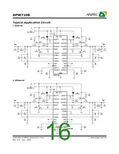
APW7108
Application Information
Output Voltage Selection
capable of carrying the required peak current without
going into saturation. In some types of inductors, es-
pecially core that is made of ferrite, the ripple cur-
rent will increase abruptly when it saturates. This
will result in a larger output ripple voltage.
The output voltage can be adjustable from 0.9V to
5.5V with a resistor-divider. Using 1% or better resistors
for the resistive divider is recommended. The VSEN
pin is the inverter input of the error amplifier, and the
reference voltage is 0.9V. Take APW7108 as the example,
the output voltage is determined by:
Output Capacitor Selection
Output voltage ripple and the transient voltage de-
viation are factors that have to be taken into consid-
eration when selecting an output capacitor. Higher
capacitor value and lower ESR reduce the output ripple
and the load transient drop. Therefore, it’s important to
select high performance low ESR capacitors that are in-
tended for switching regulator applications. In addition to
high frequency noise related MOSFET turn-on and turn-
off, the output voltage ripple includes the capaci-
tance voltage drop and ESR voltage drop caused by
the AC peak-to-peak current. These two voltages can be
represented by:
æ
ç
è
ö
÷
÷
ø
R1
ç
VOUTX = 0.9´ 1+
RGND
Where R1 is the resistor connected from VOUTX to VSENx
and RGND is the resistor connected from VSENx to the
GND.
Output Inductor Selection
The duty cycle of a buck converter is the function of the
input voltage and output voltage. Once an output voltage
is fixed, it can be written as:
VOUT
D =
V
IN
IRIPPLE
DVCOUT =
8COUTFSW
The inductor value determises the inductor ripple current
and affects the load transient reponse. Higher inductor
value reduces the inductor’s ripple current and induces
lower output ripple voltage. The ripple current and ripple
voltage can be approxminated by:
DVESR = IRIPPLE ´ RESR
These two components constitute a large portion of the
total output voltage ripple. In some applications, multiple
capacitors have to be paralleled to achieve the desired
ESR value. If the output of the converter has to support
another load with high pulsating current, more capaci-
tors are needed in order to reduce the equivalent ESR
and suppress the voltage ripple to a tolerable level. A
small decoupling capacitor in parallel for bypassing
the noise is also recommended, and the voltage rating
of the output capacitors are also must be considered.
VIN - VOUT VOUT
IRIPPLE =
´
FSW ´ L
VIN
Where FSW is the switching frequency of the regulator.
Although increase the inductor value and frequency would
reduce the ripple current and voltage, there is a tradeoff
between the inductor’s ripple current and the regulator
load transient response time.
To support a load transient that is faster than the
switching frequency, more capacitors have to be used
to reduce the voltage excursion during load step change.
Another aspect of the capacitor selection is that the
total AC current going through the capacitors has to be
less than the rated RMS current specified on the ca-
pacitors to prevent the capacitor from over-heating.
A smaller inductor will give the regulator a faster load
transient response at the expense of higher ripple
current. Increasing the switching frequency (FSW) also re-
duces the ripple current and voltage, but it will in-
crease the switching loss of the MOSFETs and the power
dissipation of the converter. The maximum ripple cur-
rent occurs at the maximum input voltage. A good starting
point is to choose the ripple current to be approximately
30% of the maximum output current. Once the induc-
tance value has been chosen, select an inductor that is
Input Capacitor Selection
The input capacitor is chosen based on the voltage rating
and the RMS current rating. For reliable operation,
Copyright ã ANPEC Electronics Corp.
20
www.anpec.com.tw
Rev. A.4 - Jan., 2009

 ANPEC [ ANPEC ELECTRONICS COROPRATION ]