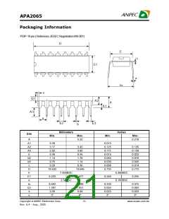
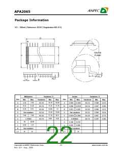
APA2065
Application Descriptions (Cont.)
Optimizing Depop Circuitry (Cont.)
volume control function abnormal when VOLUME
control signal with spike or noise. APA2065 changes
each step of volume gain after four clock cycles to
make sure control signal ready.
size of Cbypass and the turn-on time. In a SE
configuration, the output coupling capacitor, CC, is of
particular concern.
BTL Amplifier Efficiency
This capacitor discharges through the internal 10kW
resistors. Depending on the size of CC, the time
constant can be relatively large. To reduce transients
in SE mode, an external 1kW resistor can be placed in
parallel with the internal 10kW resistor. The tradeoff
for usingthisresistor isanincreaseinquiescent current.
In the most cases, choosing a small value of Ci in the
range of 0.33mF to 1mF, Cb being equal to 4.7mF and
an external 1kW resistor should be placed in parallel
with the internal 10kW resistor should produce a
virtually clickless and popless turn-on.
An easy-to-use equation to calculate efficiency starts
out asbeing equal to the ratio of power from the power
supply to the power delivered to the load.
The following equations are the basis for calculating
amplifier efficiency.
PO
PSUP
(9)
Efficiency =
Where :
PO =
VORMS x VORMS
VPxVP
=
RL
2RL
A high gain amplifier intensifies the problem as the
small delta in voltage is multiplied by the gain. So it is
advantageous to use low-gain configurations.
VP
Ö2
(10)
(11)
VORMS =
2VP
pRL
PSUP = VDD x IDDAVG = VDD x
Shutdown Function
Efficiency of a BTL configuration :
Inorder to reducepower consumption while not in use,
the APA2065 contains a shutdown pin to externally
turn off the amplifier bias circuitry. This shutdown
feature turnstheamplifier off whenalogiclowisplaced
on the SHUTDOWN pin. The trigger point between a
logic high and logic low level is typically 2.0V. It is
best to switch between ground and the supply VDD
PO
PSUP
pVP
4VDD
VPxVP ) / (VDD x 2VP ) =
(12)
(
=
2RL
pRL
Note that the efficiency of the amplifier is quite low for
lower power levels and rises sharply as power to the
loadisincreased resultingin anearlyflat internal power
dissipation over the normal operating range. Notethat
the internal dissipation at full output power is less than
in the half power range. Calculatingthe efficiency for a
specific system is the key to proper power supply
design. For a stereo 1W audio system with 8W loads
and a 5V supply, the maximum draw on the power
supply is almost 3W.
toprovidemaximum deviceperformance.
By switching the SHUTDOWNpin to low, the amplifier
enters a low-current state, IDD<50mA. On normal
operating, SHUTDOWNpin pulltohighlevel to keeping
the IC out of the shutdown mode. The SHUTDOWN
pinshouldbetiedtoadefinitevoltagetoavoidunwanted
state changes.
Afinal point toremember about linear amplifiers(either
SE or BTL) is how to manipulate the terms in the
efficiency equation to utmost advantage when
possible. Note that in equation, VDD is in the
Clock Generator
APA2065 integrates a clock block 130kHz to avoid
Copyright ã ANPEC Electronics Corp.
19
www.anpec.com.tw
Rev. A.4 - Aug., 2005

 ANPEC [ ANPEC ELECTRONICS COROPRATION ]