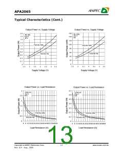
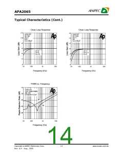
APA2065
Application Descriptions (Cont.)
Input Resistance, Ri (Cont.)
The value of Ci is important to consider as it directly
affects the low frequency performance of the circuit.
Consider the example where Ri is 10kW and the
specification calls for a flat bass response down to
100Hz. Equation is reconfigured as follow :
RF
Ri
RF
Ri
(2)
(3)
-
=
AV
SE Gain =
-2 x
=
BTL Gain
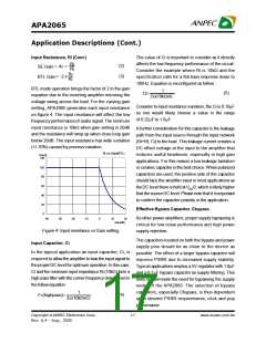
BTL mode operation brings the factor of 2 in the gain
equation due to the inverting amplifier mirroring the
voltage swing across the load. For the varying gain
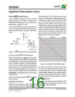
setting, APA2065 generates each input resistance
on figure 4. The input resistance will affect the low
frequency performanceof audio signal.The minmum
input resistance is 10kW when gain setting is 20dB
and the resistance will ramp up when close loop gain
below 20dB. The input resistance has wide variation
(+/-10%) caused by process variation.
1
(5)
Ci=
2px10kWxfC
Consider to input resistance variation, the Ci is 0.16mF
so one would likely choose a value in the range
of 0.22mF to 1.0mF.
Afurther consideration for this capacitor is the leakage
path from the input source through the input network
(Ri+Rf, Ci) to the load. This leakage current creates a
DC offset voltage at the input to the amplifier that
reduces useful headroom, especially in high gain
applications. For this reason a low-leakage tantalum
or ceramiccapacitor isthe best choice. When polarized
capacitors are used, the positive side of the capacitor
should face the amplifier input in most applications as
theDC level thereisheld atVDD/2, whichislikelyhigher
that thesourceDC level. Pleasenotethat it isimportant
to confirm the capacitor polarity in the application.
Ri vs Gain(BTL)
Ri(k )
W
120
100
80
60
40
20
0
Effective BypassCapacitor, Cbypass
As other power amplifiers, proper supply bypassing is
critical for low noise performance and high power
supply rejection.
-40
-30
-20
-10
0
10
20
Gain(dB)
Figure 4: Input resistance vsGain setting
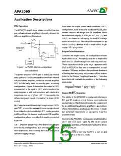
Input Capacitor, Ci
The capacitors located on both the bypass and power
supply pins should be as close to the device as
possible. The effect of a larger bypass capacitor will
improve PSRR due to increased supply stability.
Typical applicationsemploy a 5V regulator with 1.0mF
and a 0.1mF bypass capacitor as supply filtering. This
does not eliminate the need for bypassing the supply
nodes of the APA2065. The selection of bypass
capacitors, especially Cbypass, is thus dependent
upon desired PSRR requirements, click and pop
performance.
In the typical application an input capacitor, Ci, is
required to allowtheamplifier to biasthe input signal to
theproperDC level for optimum operation. In thiscase,
Ci andthe minimum input impedance Ri (10kW) form a
high-passfilter with the corner frequency determined in
thefollowequation:
1
(4)
FC(highpass)=
2px10kWxCi
Copyright ã ANPEC Electronics Corp.
17
www.anpec.com.tw
Rev. A.4 - Aug., 2005

 ANPEC [ ANPEC ELECTRONICS COROPRATION ]