APA2065
Application Descriptions (Cont.)
for power amplifier only and VDD is used for volume
Effective Bypass Capacitor, Cbypass (Cont.)
To avoid start-up pop noise occurred, the bypass
voltage should rise slower than the input bias voltage
and the relationship shown in equation (6) should be
maintained.
control amplifier and internal circuit excepting power
amplifier. The APA2065 is a high-performance
CMOS audio amplifier that requiresadequate power
supply decoupling to ensure the output total harmonic
distortion (THD) is as low as possible. Power supply
decoupling also prevents the oscillations causing by
long leadlengthbetweentheamplifier andthespeaker.
The optimum decoupling is achieved by using two
different type capacitors that target on different type
of noise on the power supply leads.
1
1
<<
(6)
Cbypass x 125kW
100kW x Ci
The bypass capacitor isfed thru from a 125kW resistor
inside the amplifier and the 100kW is maximum input
resistance of (Ri+ Rf). Bypass capacitor, Cb, values of
3.3mF to 10mF ceramic or tantalum low-ESR capacitors
are recommended for the best THD and noise
performance.
For higher frequency transients, spikes, or digital hash
on the line, a good low equivalent-series-resistance
(ESR) ceramic capacitor, typically 0.1mF placed as
close as possible to the device VDD lead works best.
For filtering lower-frequency noise signals, a large
aluminum electrolytic capacitor of 10mF or greater
placednear theaudiopoweramplifier isrecommended.
The bypass capacitance also effects to the start up
time. It is determined in the following equation:
(7)
Tstart up = 5 x (Cbypass x 125KW)
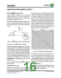
Output Coupling Capacitor, Cc
Optimizing Depop Circuitry
In the typical single-supply SE configuration, an output
coupling capacitor (Cc) is required to block the DC
bias at the output of the amplifier thus preventing DC
currentsintheload.Aswiththeinputcouplingcapacitor,
the output coupling capacitor and impedance of the
load form a high-pass filter governed by equation.
Circuitry hasbeen includedin theAPA2065to minimize
the amount of popping noise at power-up and when
coming out of shutdown mode. Popping occurs
whenever a voltage step is applied to the speaker. In
order to eliminate clicks and pops, all capacitors must
be fully discharged before turn-on. Rapid on/off
switching of the device or the shutdown function will
cause the click and pop circuitry.
1
FC(highpass)=
(8)
2pRLCC
For example, a 330mF capacitor with an 8W speaker
would attenuate low frequencies below 60.6Hz.The
main disadvantage, from a performance standpoint, is
the load impedance is typically small, which drives
the low-frequency corner higher degrading the bass
response. Large values of CC are required topass low
frequencies into the load.
The value of Ci will also affect turn-on pops (Refer to
Effective Bypass Capacitance). The bypass voltage
ramp up should be slower than input bias voltage.
Although the bypass pin current source cannot be
modified, the size of Cbypass can be changed to alter
the device turn-on time and the amount of clicks and
pops. By increasing the value of Cbypass, turn-on pop
canbereduced. However, thetradeoff for usingalarger
Power Supply Decoupling, Cs
TheAPA2065 provides two independent power inputs bypass capacitor is to increase the turn-on time for
this device. There is a linear relationship between the
for right channel and left channel used. PVDD is used
Copyright ã ANPEC Electronics Corp.
18
www.anpec.com.tw
Rev. A.4 - Aug., 2005

 ANPEC [ ANPEC ELECTRONICS COROPRATION ]