AS5050
Datasheet - Application Information
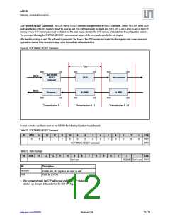
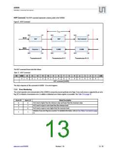
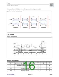
The data are sent and read with MSB first. Every time the chip is accessed it is sending and receiving data.
Figure 11. SPI Command / Response Data Flow
T
COM
MSB
LSB
MSB
LSB
MSB
LSB
MSB
LSB
MOSI
MISO
Command 1
0x00
Command 2
Response 1
Command N - 1
Response 2
Command N
Response N - 1
MSB
LSB
MSB
LSB
MSB
LSB
MSB
LSB
Transmission 1
Transmission 2
Transmission N - 1
Transmission N
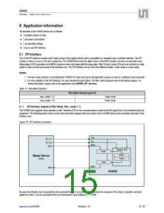
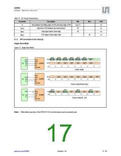
8.1.2 SPI Timing
Figure 12. SPI Timing Diagram
t XSSH
SS/
( Input )
tL
tsck
t sckL
t sckH
tH
SCK
( Input )
t MISO
tOZ
MISO
data[ 15]
data[ 14]
data[0]
( Output )
tOZ
t MOSI
MOSI
data[ 15]
data[ 14]
data[0]
( Input )
Table 16. SPI Timing Characteristics
Parameter
Description
Min
Max
Unit
ns
tOZ
tL
Time between positive edge of SS/ to output high impedance
Time between SS/ falling edge and SCK rising edge
Serial clock period
50
10
100
50
ns
tSCK
tSCKL
tSCKH
ns
Low period of serial clock
ns
High period of serial clock
50
ns
www.ams.com/AS5050
Revision 1.16
16 - 25

 AMSCO [ AMS(艾迈斯) ]