AS5050
Datasheet - Application Information
8 Application Information
The benefits of the AS5050 device are as follows:
Complete system-on-chip
Low power consumption
Low operating voltage
Easy to use SPI interface
8.1 SPI Interface
The 16-bit SPI Interface enables read / write access to the register blocks and is compatible to a standard micro controller interface. The SPI
module is active as soon as /SS pin is pulled low. The AS5050 then reads the digital value on the MOSI (master out slave in) input with every
falling edge of SCK and writes on its MISO (master in slave out) output with the rising edge. After 16 clock cycles /SS has to be set back to a high
status in order to reset some parts of the interface core. The SPI Interface can be set in two different modes: 3-wire mode or 4-wire mode.
Notes:
1. The wire mode selection is read during the POWER-UP state and can be changed with a power on reset or a software reset command.
2. For more stability on the SPI Interface, it is very important to place filters. The filter must be placed close to the driving outputs. For
further information, please refer to the application note AN5000_SPI_Interface.
Table 15. Wire Mode Selection
Wire Mode Selection (pad 14)
wire_mode = LO
wire_mode = HI
3-wire mode
4-wire mode
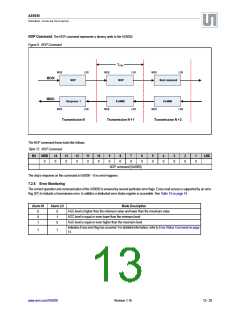
8.1.1 SPI Interface Signals (4-Wire Mode, Wire_mode = 1)
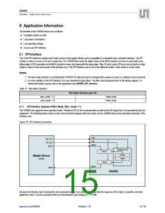
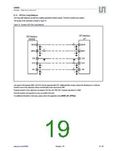
The AS5050 only supports slave operation mode. Therefore SCK for the communication as well as the /SS signal has to be provided by the test
equipment. The following picture shows a basic interconnection diagram with one master and an AS5050 device and a principle schematic of the
interface core.
Figure 10. SPI Interface Connection
SCK
SPI_CLK
SS/
SPI_SSN
MOSI
MOSI
Interface Core
RXSR
RXSPI
Master Device
(Tester)
TXSPI
TXSR
MISO
MISO
AS5050
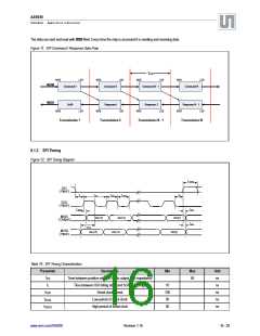
Because the interface has to decode the sent command before it can react and provide data the response of the chip to a specific command
applied at a time T can be accessed in the next transmission cycle ending at T + TCOM.
www.ams.com/AS5050
Revision 1.16
15 - 25

 AMSCO [ AMS(艾迈斯) ]