AMIS-734256, AMIS-734512, AMIS-734024
Data Sheet
25µm-pitch Wide Aperture Spectroscopic Photodiode Arrays
8.0 Clock and Voltage Requirements
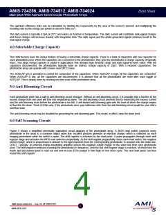
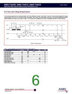
The clocking requirements are relatively simple. As it was indicated in Figure 5 and Table 1, there are only two input signals that require
clocked inputs. They are CLK, the clock for the shift register, and START, the shift register start pulse. The timing specifications and the
symbol definition for Figure 6 are listed in Table 2. The control clock amplitudes for I/Os are compatible with the 5V CMOS devices.
Figure 6: Timing Diagram
Table 2: Symbol Definitions and Timing Specifications for Timing Diagram
Item
Clock cycle time
Clock high pulse width
Clock low pulse width
Clock duty cycle
Symbol
to
twh
Min.
1000
900
100
1
Typ.
10000
Max.
Units
ns
ns
ns
twl
50
99
%
Data setup time
Data hold time
tds
tdh
telh
tehl
tsd
100
100
ns
ns
ns
ns
ns
ns
ns
EOS low-to-high delay
EOS high-to-low delay
Signal delay time
Signal settling time
Signal settle to clock edge
400
400
50
0
tsh
tsch
900
AMI Semiconductor – Aug. 06, M-20603-001
6
www.amis.com

 AMI [ AMI SEMICONDUCTOR ]