AMIS-734256, AMIS-734512, AMIS-734024
Data Sheet
25µm-pitch Wide Aperture Spectroscopic Photodiode Arrays
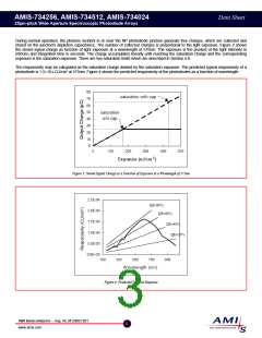
The quantum efficiency (QE) can be calculated by dividing the responsivity by the area of the sensor's element and multiplying the
resulting ratio by the energy per photon in electron volts (eV).
The dark current is typically 0.2pA at 25°C and varies as function of temperature. The dark current will contribute dark-signal charges
and these charges will increase linearly with integration time. The dark signal and the photo-generated signal combined result in the
total signal charge.
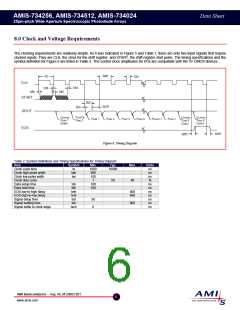
4.0 Selectable Charge Capacity
The HSN devices have the unique feature of having a selectable charge capacity. There is a bank of capacitors with one capacitor for
each photodiode pixel. When the capacitors are connected to the photodiodes, they give the photodiodes a charge capacity of typically
65pC. This large charge capacity is useful in applications that demand high dynamic range and high signal-to-noise ratios. With the
capacitors disconnected, the photodiodes typically have an intrinsic charge capacity of 25pC. With a reduced capacitance, the
photodiode array can operate with a lower reset (kTC) noise.
The ADDCAP pin is provided to control the connection of the capacitors. When ADDCAP is high, all the capacitors are connected.
When ADDCAP is low, all the capacitors are disconnected. It is advised that all the photodiodes are reset after each toggle of
ADDCAP. This is simply done by clocking one line scan of the photodiode array.
5.0 Anti-Blooming Circuit
Each photodiode pixel has a built-in anti-blooming circuit structure. Without an anti-blooming circuit, it is possible that a fraction of the
excess charge from one pixel will flow into neighboring pixels. The anti-blooming circuit prevents this by redirecting the excess current
into the anti-blooming drain before the photodiode is too full. A self-biased anti-blooming gate sets the level at which the charge begins
to flow into the drain. Think of it this way. If the photodiode were your bathroom sink, then the anti-blooming circuit would be your sink’s
overflow drain.
The anti-blooming circuit may be disabled by grounding the anti-blooming gate. This would, in effect, raise the drain level.
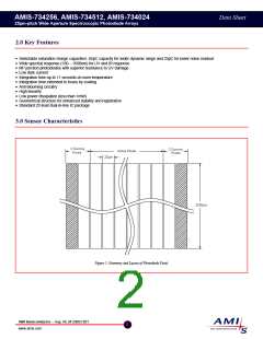
6.0 Self-Scanning Circuit
Figure 5 shows a simplified electrically equivalent circuit diagram of the photodiode array. A MOS read switch connects every
photodiode in the array to a common output video line. Incident photons generate an electron charge, which is collected on each
imaging photodiode while the switch is open. The shift register is activated by the start pulse. A pulse propagates through each shift
register stage and activates the MOS read switches sequentially. As the shift register sequentially closes each read switch, the negative
stored charge, which is proportional in amount to the light exposure from the corresponding photodiode, is readout onto the video line,
QOUT. Typically, an external charge-integrating amplifier senses the negative output charge on the video line from each photodiode
pixel. The shift register continues scanning the photodiodes in sequence, until the last shift register stage is reached, at which time the
fourth and last dummy pixel is read out and end-of-scan (EOS) output is held high for one clock cycle. The next start pulse can then
restart the shift register.
AMI Semiconductor – Aug. 06, M-20603-001
4
www.amis.com

 AMI [ AMI SEMICONDUCTOR ]