AMIS-734256, AMIS-734512, AMIS-734024
Data Sheet
25µm-pitch Wide Aperture Spectroscopic Photodiode Arrays
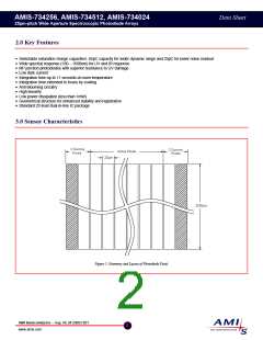
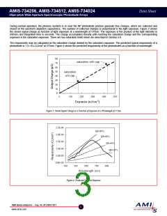
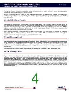
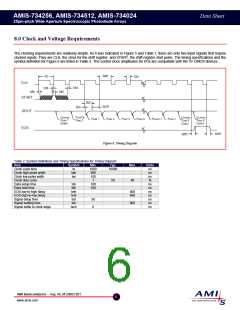
Figure 5: Simplified Circuit Diagram of an HSN Photodiode Array
The diagram in Figure 5 does not include the capacitor bank and the anti-blooming circuitry.
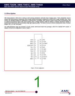
7.0 I/O Pins
Besides the VSS and VDD supply pins, there are nine functionally active I/O pins. Only two clocks, CLK and START, are required for
controlling the timing of the sensor's video readout. One additional digital input, ADDCAP controls the bank of capacitors as described
in the Section 6.0. The digital output, EOS, marks the end of the line-scan. The charge output pin, QOUT, is typically connected to a
charge-integrating amplifier, which is biased to Vbias (see Section 8.0). For normal anti-blooming operation, the ABG requires a 0.1µF
capacitor connected to VSS and the ABD is also biased to Vbias. Each temperature diode is operated with a small constant current,
which forward biases its PN junction. By measuring the forward-bias voltage, one can track the silicon die temperature. The
temperature diodes may be disabled by connecting their anodes to VSS. These I/Os are listed with their acronym designators and
functional descriptions in Table 1.
Table 1: Symbols and Functions and I/O Pins
Symbol
VSS
Function and Description
Ground
VDD
+5.0V
START
CLK
Start pulse: input to start the line scan
Clock pulse: input to clock the shift register
ADDCAP
EOS
QOUT
ABG
ABD
TD1
Add capacitors: input that selects the bank of capacitors to increase charge capacity
End of scan: output from the shift register to indicate the completion of one line scan
Video charge output: output from the photodiodes pixels
Anti-blooming gate: self-biased gate for setting anti-blooming level. Requires 0.1-µF connected to VSS
Anti-blooming drain: bias for anti-blooming drain, set to Vbias
Temperature Diode 1: anode of temperature Diode 1
Temperature Diode 2: anode of temperature Diode 2
No connection
TD2
NC
AMI Semiconductor – Aug. 06, M-20603-001
5
www.amis.com

 AMI [ AMI SEMICONDUCTOR ]