AMD
P R E L I M I N A R Y
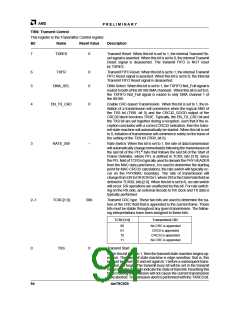
TIR11: Transmit Sequence Control
This register is the Transmit Sequence Control. The
bits in this register determine the function of the transmit
sequence signals.
Bit
Name
Reset Value
Description
7
RXCD
pin
RXC/IRQ10 pin Data. The value that is written to this bit will be
driven out to the RXC pin when the RXCEN bit of TCR15 has been
set to a 1 and the RXCFN bit of TCR28 has been set to a 0.
The value that is read from RXCD represents the current value of
the RXC/IRQ10 pin. The control of the function of the RXC/IRQ10
pin is described in the Multi-Function Pin section.
6
5
4
USER6D
USER5D
LLOCKE
pin
pin
pin
USER6/IRQ5 pin Data. The value that is written to USER6D may be
driven out to the USER6/IRQ5 pin, depending upon the values of
the USER6EN bit (TCR15[3]), the USER6FN bit (TCR7[6]), the ISA
PnP registers 70h and 71h, and the operating mode of the
Am79C930 device.
The value read from USER6D will always represent the current
value of the USER6/IRQ5 pin. The control of the function of the
USER6/IRQ5 pin is described in the Multi-Function Pin section.
USER5/IRQ4 pin Data. The value that is written to USER5D may be
driven out to the USER5/IRQ4 pin, depending upon the values of
the USER5EN bit (TCR15[2]), the USER5FN bit (TCR7[5]), the ISA
PnP registers 70h and 71h, and the operating mode of the
Am79C930 device.
The value read from USER5D will always represent the current
value of the USER5/IRQ4 pin. The control of the function of the
USER5/IRQ4 pin is described in the Multi-Function Pin section.
LLOCKE pin data value. The value that is written to LLOCKE may
be driven out to the LLOCKE/SA15 pin, depending upon the values
of the LLOCKEN bit (TCR14[6]), and the operating mode of the
Am79C930 device (i.e., PCMCIA or ISA).
The value read from LLOCKE will always represent the current
value of the LLOCKE/SA15 pin. The control of the function of the
LLOCKE/SA15 pin is described in the Multi-Function Pin section.
3
2
RCEN
0
0
Register Control Enable. Used to control the functional timing of
the TXCMD, TXMOD and TXPE pin values as defined in the
Multi-Function Pin section. See the Multi-Function Pin section de-
scription for each of these pins for more details.
TXMOD
TXMOD pin control. Used to control the functional timing of the
TXCMD, pin value as defined in the Multi-Function Pin section. See
the Multi-Function Pin section description for more details.
1
0
TXPE
0
0
TXPEpin control. The TXPE bit affects the value of theTXPEpin as
described in the Multi-Function Pin section.
TXCMD
TXCMD and TXCMD pin control. The TXCMD bit affects the value
of the the TXCMD andTXCMD pins as described in theMulti-Func-
tion Pin section.
96
Am79C930

 AMD [ AMD ]