AMD
P R E L I M I N A R Y
The following is a brief summary of the IEEE 1149.1
compatible test functions implemented in the
Am79C930 device:
TAP FSM
The TAP engine is a 16-state FSM, driven by the Test
Clock (TCK) and the Test Mode Select (TMS) pins. This
FSM is in its reset state at power up or after H_RESET.
The TRST pin is supported in order to ensure that the
FSM is in the TEST_LOGIC_RESET state before test-
ing is begun.
Boundary Scan Circuit
The boundary scan test circuit uses five pins: TRST,
TCK, TMS, TDI, and TDO. These five pins are collec-
tively labeled the TAP. The boundary scan test circuit in-
cludes a finite state machine (FSM), an instruction
register, and a data register array. Internal pull-up resis-
torsareprovidedfortheTDIandTMSpins. TheTCKpin
must not be left unconnected.
Supported Instructions
In addition to the minimum IEEE 1149.1 requirements
(BYPASS, EXTEST, and SAMPLE instructions), one
additional instruction (IDCODE) is provided as addi-
tional support for board level testing. All unused instruc-
tion decodes are reserved.
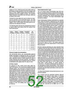
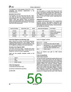
Instruction Name
Instruction Code
Mode
Selected Data Register
Description
EXTEST
ID_CODE
SAMPLE
Reserved
BYPASS
0000
0001
Test
BSR
ID
External Test
Normal
Normal
Reserved
Normal
REG ID Code Inspection
Sample Boundary
Reserved
0010
BSR
0011–1110
1111
Reserved
Bypass
Bypass Scan
Instruction Register and Decoding Logic
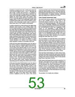
Device ID Register Contents:
After H_RESET or S_RESET, the IDCODE instruction
is always loaded into the IEEE 1149.1 register. The de-
coding logic gives signals to control the data flow in the
DATA registers according to the current instruction.
Bits 31–28:
Bits 27–12:
Bits 11–1:
Version
Part Number (0010 1000 0101 0000)
Manufacturer ID. The 11 bit manufacturer
ID code for AMD is 00000000001 in accor-
dance with JEDEC publication 106-A.
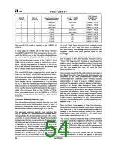
Boundary Scan Register (BSR)
Each BSR cell has two stages. A flip-flop and a latch
are used for the SERIAL SHIFT STAGE and for the
PARALLEL OUTPUT STAGE, respectively.
Bit 0:
Always a logic 1
This is an internal scan path for AMD internal
testing use.
There are four possible operation modes in the
BSR cell:
Power Saving Modes
Power Down Function
1
2
3
4
Capture
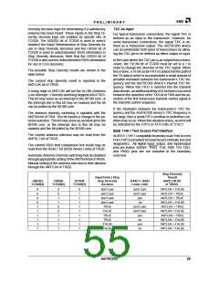
TheAm79C930BIUincludesfiveregistersthatareused
to invoke a power-down function that will support the
IEEE 802.11 (draft) specified power down by allowing
variable lengths of power-down and power-up time. The
registers include the Processor Interface Register
(MIR0), which contains the Power Down command bit, a
Power Down Length Count set of registers (MIR2,3,4),
and a Power Up Clock Timer (MIR1) register. The power
down sequence is executed by the firmware running
on the embedded 80188, either independently, or in
response to a request from the host. In the PCMCIA
Shift
Update
System Function
Other Data Registers
(1) BYPASS REGISTER (1 BIT)
(2) DEVICE ID REGISTER (32 BITS)
(3) INSCAN0
56
Am79C930

 AMD [ AMD ]